What is BGA Soldering?
BGA soldering is a process that involves attaching a BGA component to a PCB using a grid of solder balls pre-attached to the bottom of the component package. The solder balls are arranged in a matrix pattern, allowing for a high density of interconnections between the component and the PCB.
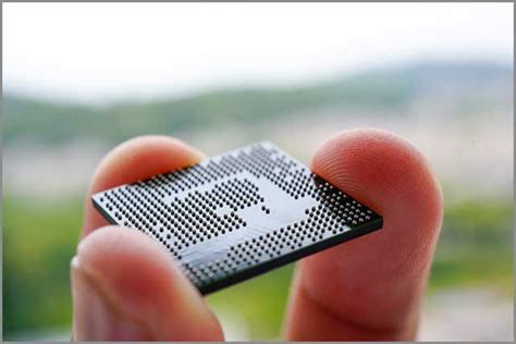
The BGA package consists of a substrate with a grid of pads on the bottom side, each connected to a corresponding pad on the top side through vias. The top side of the substrate is where the integrated circuit (IC) is mounted. The solder balls are attached to the pads on the bottom side of the substrate, forming the connection between the BGA package and the PCB.
Advantages of BGA Soldering
- High interconnection density
- Improved electrical and thermal performance
- Smaller package size
- Better signal integrity
- Reduced lead inductance
Disadvantages of BGA Soldering
- Difficulty in inspection and rework
- Higher cost of equipment and materials
- Requires precise alignment and placement
- Thermal management challenges
The BGA Soldering Process
The BGA soldering process involves several steps, each critical for achieving reliable solder joints. Here’s a breakdown of the process:
1. PCB Preparation
Before soldering the BGA component, the PCB must be properly prepared. This includes:
- Cleaning the PCB to remove any contaminants or debris
- Applying solder paste to the PCB pads using a stencil or solder paste printer
- Inspecting the solder paste application for consistency and accuracy
2. BGA Component Placement
Once the PCB is prepared, the BGA component is placed onto the solder paste-covered pads. This process requires precise alignment and placement, often achieved using specialized pick-and-place equipment.
3. Reflow Soldering
After the BGA component is placed, the PCB undergoes reflow soldering. This process involves heating the PCB and component in a controlled manner to melt the solder paste and form the solder joints. The reflow soldering process typically follows a specific temperature profile, which includes:
- Preheat: The PCB and component are gradually heated to activate the flux and evaporate solvents.
- Soak: The temperature is maintained to allow the component and PCB to reach thermal equilibrium.
- Reflow: The temperature is increased above the melting point of the solder, allowing the solder to flow and form the joints.
- Cooling: The PCB and component are cooled down gradually to solidify the solder joints.
4. Inspection and Testing
After the reflow soldering process, the PCB undergoes inspection and testing to ensure the quality and reliability of the solder joints. This may include:
- Visual inspection using microscopes or cameras
- X-ray inspection to check for voids, shorts, or opens
- Electrical testing to verify functionality and performance

BGA Soldering Equipment
To successfully perform BGA soldering, several pieces of equipment are essential:
1. Stencil Printer
A stencil printer is used to apply solder paste to the PCB pads. The stencil is a thin metal sheet with apertures that match the pad layout on the PCB. The solder paste is forced through the apertures onto the pads, ensuring a consistent and accurate application.
2. Pick-and-Place Machine
A pick-and-place machine is used to accurately place the BGA component onto the solder paste-covered pads on the PCB. These machines use vision systems and precise motion control to align and place the component with high accuracy.
3. Reflow Oven
A reflow oven is used to perform the reflow soldering process. These ovens have multiple heating zones that can be programmed to follow a specific temperature profile, ensuring proper melting and solidification of the solder joints.
4. Inspection Equipment
Inspection equipment, such as microscopes, cameras, and X-ray machines, is used to verify the quality and reliability of the solder joints after the reflow process.

Challenges in BGA Soldering
BGA soldering presents several challenges that must be addressed to ensure reliable and robust solder joints:
1. Thermal Management
BGA packages have a high thermal mass, which can lead to uneven heating during the reflow process. This can result in poor solder joint formation or even component damage. Proper thermal management, including the use of thermally conductive materials and optimized reflow profiles, is essential.
2. Warpage and Coefficient of Thermal Expansion (CTE) Mismatch
Differences in the CTE between the BGA package and the PCB can lead to warpage during the reflow process. This can cause open or weak solder joints. Using materials with similar CTEs and implementing proper PCB design techniques can help mitigate this issue.
3. Voiding
Voids, or air pockets, within the solder joints can reduce their strength and reliability. Voids can be caused by various factors, such as improper solder paste application, incorrect reflow profiles, or contamination. Optimizing the soldering process and using materials that minimize voiding is crucial.
4. Rework and Repair
Reworking or repairing BGA solder joints can be challenging due to the difficulty in accessing the solder balls underneath the package. Specialized equipment, such as hot air rework stations and BGA reballing kits, may be required for successful rework.

Best Practices for BGA Soldering
To ensure reliable and robust BGA solder joints, follow these best practices:
- Use a well-designed PCB with proper pad sizes, spacing, and solder mask openings.
- Select compatible materials, including the BGA package, PCB substrate, and solder paste.
- Implement a precise and consistent solder paste application process.
- Ensure accurate alignment and placement of the BGA component.
- Optimize the reflow soldering profile for the specific BGA package and PCB materials.
- Perform thorough inspection and testing to verify solder joint quality and reliability.
- Follow proper handling and storage procedures for BGA components and PCBs.
Frequently Asked Questions (FAQ)
1. What is the difference between BGA and QFN packages?
BGA packages have a grid of solder balls underneath the package, while QFN (Quad Flat No-lead) packages have peripheral pads around the edges of the package. BGA packages offer higher interconnection density and better thermal performance compared to QFN packages.
2. Can BGA components be soldered using hand soldering techniques?
Hand soldering BGA components is not recommended due to the small size of the solder balls and the difficulty in accessing them underneath the package. Reflow soldering using specialized equipment is the preferred method for BGA soldering.
3. What is the purpose of solder paste in BGA soldering?
Solder paste is a mixture of tiny solder particles suspended in flux. It is applied to the PCB pads before placing the BGA component. During the reflow soldering process, the solder particles melt and form the solder joints between the BGA package and the PCB.
4. How can voids in BGA solder joints be minimized?
Voids in BGA solder joints can be minimized by optimizing the solder paste application process, using a proper reflow soldering profile, and selecting compatible materials. Using solder paste with a fine particle size and low oxide content can also help reduce voiding.
5. What is the role of flux in BGA soldering?
Flux is a chemical compound that helps remove oxides and other contaminants from the surfaces of the solder balls and PCB pads during the soldering process. It also promotes the flowing and wetting of the solder, ensuring the formation of reliable solder joints. The flux is activated during the preheat and soak stages of the reflow soldering profile.
Conclusion
BGA soldering is a critical process in the assembly of modern electronic devices, offering numerous advantages over traditional packaging techniques. However, it also presents unique challenges that must be addressed through proper equipment, materials, and processes.
By understanding the basics of BGA soldering, following best practices, and staying up-to-date with the latest advancements in the field, engineers and technicians can ensure the production of high-quality, reliable electronic assemblies that meet the ever-increasing demands of the industry.


Leave a Reply