Introduction to Low-noise Amplifiers
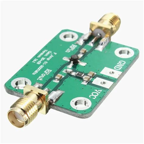
A low-noise amplifier (LNA) is an electronic amplifier used to amplify very weak signals captured by an antenna. It is usually located very close to the antenna to minimize losses in the feedline. LNAs are a key component in many radio communications systems, including cellular networks, GPS receivers, satellite communications, and radar systems.
The main purpose of an LNA is to amplify weak signals while adding as little noise and distortion as possible, thus improving the receiver’s sensitivity. The noise figure (NF) is a key parameter that quantifies the noise added by the LNA to the signal. A lower NF means better performance.
Key Parameters of Low-noise Amplifiers
| Parameter | Description |
|---|---|
| Noise Figure (NF) | The ratio of the signal-to-noise ratio (SNR) at the input to the SNR at the output, expressed in dB. A lower NF is better. |
| Gain | The ratio of the output signal power to the input signal power, expressed in dB. Higher gain is generally better. |
| Linearity | The ability of the amplifier to produce an output signal that is a linear function of the input signal. Nonlinearity causes distortion. |
| Input and Output Return Loss | A measure of how well the amplifier is matched to the source and load impedances. Higher return loss (in dB) is better. |
| Stability | The ability of the amplifier to avoid self-oscillation. Unconditional stability is desired. |
| Power Consumption | The DC power required by the amplifier. Lower power consumption is preferred, especially in battery-powered applications. |
Tip 1: Choose the Right Transistor Technology
The choice of transistor technology is critical in LNA design. The most common technologies are:
- Silicon Bipolar Junction Transistors (BJTs)
- Silicon Germanium (SiGe) Heterojunction Bipolar Transistors (HBTs)
- Gallium Arsenide (GaAs) High Electron Mobility Transistors (HEMTs)
Each technology has its strengths and weaknesses, as summarized in the table below:
| Technology | Advantages | Disadvantages |
|---|---|---|
| Si BJT | Low cost, widely available | Higher NF, lower gain, lower frequency limit |
| SiGe HBT | Lower NF and higher gain than Si BJT, higher frequency limit, lower cost than GaAs | Higher cost than Si BJT |
| GaAs HEMT | Lowest NF, highest gain, highest frequency limit | Highest cost, more complex fabrication |
For most applications below 10 GHz, SiGe HBTs offer the best combination of performance and cost. For very high frequency applications or the lowest possible NF, GaAs HEMTs are preferred.

Tip 2: Optimize the Noise Matching
The noise figure of an LNA is determined by the noise contributed by the transistor and the impedance matching at the input. Noise matching involves selecting the source impedance that minimizes the NF.
The optimal source impedance for noise matching is generally different from the impedance that provides the maximum power transfer (conjugate matching). Therefore, there is a trade-off between noise figure and gain.
There are several techniques for noise matching:
-
Feedback: A small amount of degenerative feedback can be used to adjust the input impedance for noise matching. This technique is simple but may degrade the NF and gain.
-
Inductive Degeneration: A series inductance in the emitter/source of the transistor can be used to provide a real term in the input impedance without adding noise. This technique is widely used in narrowband LNAs.
-
Balanced/Differential Design: A balanced LNA configuration can provide a good compromise between noise figure and input matching. The input signal is split into two anti-phase components, amplified separately, and then combined. This doubles the effective transconductance, improving the gain and NF.

Tip 3: Use Inductive Degeneration for Simultaneous Noise and Input Matching
Inductive degeneration is a powerful technique that allows simultaneous noise and input matching in a narrow frequency band. The key is to choose the inductance value that provides the desired real part of the input impedance for noise matching while resonating out the imaginary part for power matching.
The input impedance of an inductively degenerated common-emitter stage is given by:
Z_in = (gm * Ls) / Cπ + jω(Ls + Lg) + 1/jωCπ
Where:
– gm is the transistor transconductance
– Ls is the emitter degeneration inductance
– Lg is the gate inductance
– Cπ is the base-emitter capacitance
By choosing Ls and Lg appropriately, the real and imaginary parts of Z_in can be made equal to the optimal source impedance for noise matching and power matching respectively, at the frequency of interest.

Tip 4: Use a Cascode Configuration for Higher Gain and Stability
The cascode configuration consists of a common-emitter stage followed by a common-base stage. It has several advantages over a single common-emitter stage:
-
Higher Gain: The Miller effect, which limits the gain of a common-emitter stage, is greatly reduced in a cascode. This allows higher gain to be achieved.
-
Higher Bandwidth: The reduced Miller capacitance also allows a higher bandwidth to be achieved for a given gain.
-
Higher Output Impedance: The common-base stage presents a high impedance load to the common-emitter stage, increasing the overall output impedance. This is beneficial for output matching.
-
Improved Stability: The cascode configuration is inherently more stable than a single common-emitter stage due to the reduced feedback from output to input.
The main disadvantage of the cascode is the higher voltage headroom required, as the supply voltage is split between the two transistors. This can be an issue in low-voltage designs.
Tip 5: Use a π-Network for Wideband Input Matching
For wideband LNAs, the narrowband noise matching techniques described earlier are not sufficient. A common approach for wideband input matching is to use a π-network.
A π-network consists of two series inductors and one shunt capacitor (or vice versa). By choosing the component values appropriately, a good match to the source impedance can be achieved over a wide frequency range.
The design of the π-network involves trade-offs between the bandwidth, the noise figure, and the input return loss. In general, a higher inductance value provides a better match but a narrower bandwidth.
A common variant of the π-network is the split-inductor network, where the series inductor is split into two parts with the shunt capacitor in between. This provides an additional degree of freedom in the design and can help to improve the noise figure.
Tip 6: Use Negative Feedback for Linearity and Stability
While an LNA’s primary focus is on noise figure and gain, linearity and stability are also important considerations. Negative feedback can be used to improve both of these parameters.
Negative feedback involves taking a portion of the output signal and feeding it back to the input in anti-phase. This has several effects:
-
Reduced Gain: Feedback reduces the overall gain of the amplifier. While this may seem counterproductive, it can be necessary to achieve the desired linearity and stability.
-
Improved Linearity: Negative feedback reduces distortion by correcting for nonlinearities in the amplifier’s transfer characteristic.
-
Improved Stability: Negative feedback can improve stability by reducing the effect of parameter variations with temperature and frequency.
The amount of feedback is a design trade-off. More feedback provides better linearity and stability but reduces the gain and potentially increases the noise figure.
Common feedback topologies in LNAs include series-shunt feedback and parallel-series feedback. The choice depends on the specific design requirements.
Tip 7: Consider Balanced/Differential Design for Best Performance
Balanced or differential LNA designs offer several advantages over single-ended designs:
-
Improved Noise Figure: The effective transconductance of a differential pair is twice that of a single transistor, resulting in a 3 dB improvement in noise figure.
-
Rejection of Common-mode Noise: Differential designs are inherently resistant to common-mode noise, such as power supply noise or interference picked up by the antenna.
-
Easier Matching: The input and output of a differential LNA are balanced, which simplifies the design of matching networks.
-
Higher Linearity: Nonlinearities in the two halves of a differential pair tend to cancel each other out, resulting in improved linearity.
The main disadvantage of a differential design is the increased complexity and component count. Baluns (balanced-to-unbalanced transformers) are required at the input and output to interface with single-ended systems.
Despite the increased complexity, the performance benefits of differential LNAs make them the preferred choice in many high-performance applications.
FAQ
1. What is the difference between an LNA and a regular amplifier?
An LNA is a specialized type of amplifier designed to amplify very weak signals while adding minimal noise. In contrast, a regular amplifier is designed for larger signals and its noise performance is less critical. LNAs are typically used in the early stages of a receiver chain, close to the antenna, while regular amplifiers are used later in the chain.
2. Why is noise figure important in an LNA?
The noise figure is a key performance metric for LNAs because it directly impacts the sensitivity of the receiver. A lower noise figure means that weaker signals can be detected and processed. In applications like radio astronomy or deep space communications, where the signals are extremely weak, a low noise figure is critical.
3. What is the trade-off between noise figure and gain in an LNA?
There is a fundamental trade-off between noise figure and gain in an LNA. The impedance match for minimum noise figure is different from the match for maximum gain. LNA designs must strike a balance between these two parameters based on the specific application requirements.
4. What is the purpose of inductive degeneration in an LNA?
Inductive degeneration is a technique used in LNAs to provide simultaneous noise and power matching. A series inductor in the emitter/source of the transistor introduces a real term in the input impedance without adding noise. By choosing the inductance value appropriately, the input can be matched for both noise and power at a specific frequency.
5. Why are differential LNA designs preferred in high-performance applications?
Differential LNAs offer several advantages over single-ended designs, including better noise figure, rejection of common-mode noise, easier matching, and higher linearity. While they are more complex and require more components, the performance benefits make them the preferred choice in demanding applications like cellular base stations and satellite receivers.
Conclusion
The design of low-noise amplifiers involves a complex trade-off between noise figure, gain, linearity, stability, and bandwidth. The key to a successful LNA design is a deep understanding of these trade-offs and the ability to choose the right techniques for the specific application.
The seven tips covered in this article – choosing the right transistor technology, optimizing noise matching, using inductive degeneration, using a cascode configuration, using a π-network for wideband matching, using negative feedback, and considering differential design – provide a solid foundation for LNA design.
However, LNA design is a vast and constantly evolving field. As new technologies and techniques emerge, designers must stay up-to-date to create amplifiers that push the boundaries of performance. With the right knowledge and tools, engineers can design LNAs that enable new applications and advance the state of the art in radio communications.


Leave a Reply