Introduction to SMT and SMD
In the world of electronic manufacturing, particularly in the realm of printed circuit boards (PCBs), there are numerous terms and acronyms that can be confusing for those new to the industry. Two of the most commonly used and often misunderstood terms are SMT (Surface Mount Technology) and SMD (Surface Mount Device). While they may sound similar, they refer to different aspects of the PCB assembly process. In this comprehensive guide, we will delve into the intricacies of SMT and SMD, explaining their differences, applications, and the role they play in modern electronics manufacturing.
What is Surface Mount Technology (SMT)?
Surface Mount Technology (SMT) is a method of assembling electronic components directly onto the surface of a printed circuit board (PCB). This technology has revolutionized the electronics industry since its introduction in the 1960s, enabling the production of smaller, faster, and more reliable electronic devices. SMT has largely replaced the older through-hole technology (THT), which involved inserting component leads through holes in the PCB and soldering them on the opposite side.
The SMT process involves several key steps:
-
Solder Paste Application: A precise amount of solder paste, a mixture of tiny solder particles and flux, is applied to the PCB’s contact pads using a stencil or screen printing process.
-
Component Placement: Surface mount devices (SMDs) are precisely placed onto the solder paste-covered pads using automated pick-and-place machines or, in some cases, by hand.
-
Reflow Soldering: The PCB with the placed components is then passed through a reflow oven, which heats the board to a specific temperature profile, melting the solder particles and forming a strong electrical and mechanical bond between the components and the PCB.
-
Inspection and Testing: After the soldering process, the assembled PCBs undergo visual inspection and various electrical tests to ensure the quality and functionality of the final product.
SMT offers several advantages over through-hole technology:
- Miniaturization: SMDs are much smaller than their through-hole counterparts, allowing for higher component density and more compact PCB designs.
- Faster Assembly: Automated SMT processes enable faster placement and soldering of components, reducing overall production time.
- Cost-Effectiveness: The increased automation and reduced manual labor in SMT lead to lower manufacturing costs, especially for high-volume production.
- Improved Reliability: SMT provides better mechanical and thermal stress resistance, resulting in more reliable electronic assemblies.
What are Surface Mount Devices (SMDs)?
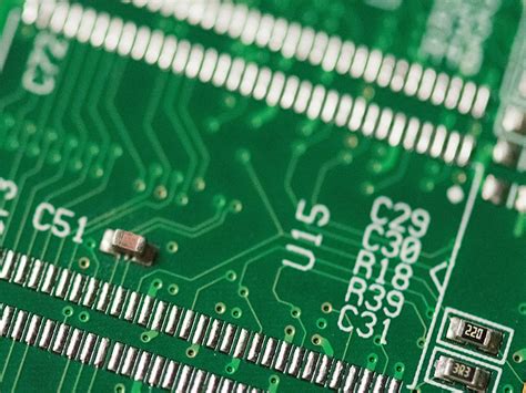
Surface Mount Devices (SMDs) are electronic components designed specifically for use in Surface Mount Technology (SMT) assembly processes. These components are mounted directly onto the surface of a printed circuit board (PCB) without the need for through-holes. SMDs come in various package types and sizes, each with its own set of characteristics and applications.
Common SMD package types include:
- Resistors and Capacitors:
- Chip resistors and capacitors (e.g., 0402, 0603, 0805, 1206)
-
MELF (Metal Electrode Leadless Face) resistors and capacitors
-
Inductors:
- Chip inductors (e.g., 0402, 0603, 0805, 1206)
-
Wirewound inductors
-
Integrated Circuits (ICs):
- Small Outline Integrated Circuit (SOIC)
- Thin Small Outline Package (TSOP)
- Quad Flat Package (QFP)
- Ball Grid Array (BGA)
-
Quad Flat No-Lead (QFN)
-
Transistors and Diodes:
- Small Outline Transistor (SOT)
- Small Outline Diode (SOD)
-
Thin Small Outline Package (TSOP)
-
Connectors:
- Surface mount headers and sockets
- Edge connectors
- USB, HDMI, and other interface connectors
SMDs offer several advantages over through-hole components:
- Smaller Size: SMDs are much smaller than through-hole components, enabling higher component density and more compact PCB designs.
- Reduced Weight: The smaller size and absence of leads in SMDs contribute to an overall reduction in the weight of the electronic assembly.
- Improved High-Frequency Performance: SMDs have shorter leads and smaller parasitic capacitances and inductances, making them more suitable for high-frequency applications.
- Automated Assembly: SMDs are designed for automated pick-and-place machines, allowing for faster and more efficient assembly processes.
Differences between SMT and SMD
While SMT and SMD are closely related terms, they refer to different aspects of the PCB assembly process. The main differences between SMT and SMD are:
- Definition:
- SMT (Surface Mount Technology) refers to the process and techniques used to assemble electronic components onto the surface of a PCB.
-
SMD (Surface Mount Device) refers to the actual electronic components that are designed for use in the SMT assembly process.
-
Scope:
- SMT encompasses the entire assembly process, including solder paste application, component placement, reflow soldering, and inspection.
-
SMD focuses on the physical characteristics and package types of the electronic components used in the SMT process.
-
Application:
- SMT is a manufacturing process that is widely used in the electronics industry for assembling PCBs.
- SMDs are the building blocks used in the SMT process to create the desired electronic circuits and functionality.
In summary, SMT is the technology and process used to assemble PCBs, while SMDs are the components specifically designed for use in the SMT process.

Advantages of SMT and SMD in PCB Assembly
The adoption of Surface Mount Technology (SMT) and Surface Mount Devices (SMDs) has brought about numerous advantages in the PCB assembly process. These advantages have driven the widespread use of SMT and SMDs in the electronics industry, enabling the production of smaller, faster, and more reliable electronic devices. Some of the key advantages include:
- Miniaturization and High Component Density:
- SMDs are significantly smaller than through-hole components, allowing for higher component density on PCBs.
- Smaller component sizes enable the design of more compact and lightweight electronic devices.
-
Increased component density leads to more efficient use of PCB real estate, reducing overall product size.
-
Faster Assembly and Increased Automation:
- SMT is highly automated, utilizing pick-and-place machines for precise and rapid component placement.
- Automated assembly processes result in faster production times and higher throughput compared to manual through-hole assembly.
-
Increased automation reduces the risk of human error and improves overall assembly quality and consistency.
-
Cost-Effectiveness:
- The automation and speed of SMT processes lead to lower labor costs and reduced assembly time.
- Higher component density allows for more efficient use of PCB materials, reducing material costs.
-
Fewer drilling operations are required for SMDs, further reducing manufacturing costs.
-
Improved Reliability and Performance:
- SMDs have shorter leads and smaller parasitic capacitances and inductances, resulting in improved high-frequency performance.
- The absence of through-holes in SMT reduces the risk of board delamination and improves the mechanical strength of the PCB.
-
SMT provides better thermal and mechanical stress resistance, enhancing the overall reliability of the electronic assembly.
-
Design Flexibility:
- SMT allows for the placement of components on both sides of the PCB, enabling more complex and space-efficient designs.
- The wide variety of SMD package types and sizes offers designers greater flexibility in component selection and PCB layout.
-
SMT facilitates the integration of advanced packaging technologies, such as Ball Grid Arrays (BGAs) and Chip Scale Packages (CSPs).
-
Environmental Benefits:
- SMT requires less solder material compared to through-hole technology, reducing the environmental impact of lead-based solders.
- The smaller size of SMDs results in less electronic waste and a reduced environmental footprint.
- The elimination of through-holes in SMT reduces the need for drilling operations, minimizing the generation of hazardous dust and debris.
The advantages of SMT and SMD have revolutionized the electronics industry, enabling the production of smaller, faster, and more reliable electronic devices while reducing costs and environmental impact. As technology continues to advance, SMT and SMD will remain integral to the development and manufacturing of cutting-edge electronic products.

Challenges and Considerations in SMT and SMD Assembly
While Surface Mount Technology (SMT) and Surface Mount Devices (SMDs) offer numerous advantages in PCB assembly, there are also several challenges and considerations that manufacturers and designers must address to ensure successful and reliable electronic assemblies. Some of these challenges and considerations include:
- Component Placement Accuracy:
- Accurate placement of SMDs is critical for proper electrical connections and overall assembly quality.
- High-precision pick-and-place machines and vision systems are required to achieve the necessary placement accuracy, especially for small and fine-pitch components.
-
Proper machine calibration, maintenance, and operator training are essential to minimize placement errors.
-
Solder Paste Printing:
- Consistent and precise solder paste deposition is crucial for forming reliable solder joints.
- Factors such as stencil design, aperture size, and solder paste properties must be carefully considered to achieve optimal solder paste printing results.
-
Regular stencil cleaning and maintenance are necessary to prevent solder paste contamination and ensure consistent print quality.
-
Reflow Soldering Process Control:
- The reflow soldering process must be carefully controlled to achieve proper solder joint formation and avoid defects such as bridging, tombstoning, or insufficient wetting.
- Proper reflow oven temperature profiling and monitoring are essential to ensure that the solder paste reaches the correct temperature and time for optimal melting and solidification.
-
Moisture sensitivity of SMDs must be considered, and appropriate measures, such as baking or dry storage, should be taken to prevent moisture-related defects during reflow.
-
Thermal Management:
- SMDs, especially high-power components, generate heat during operation, which must be efficiently dissipated to ensure reliable performance and prevent premature failure.
- Proper PCB layout, thermal vias, and heat sinks must be incorporated into the design to facilitate heat dissipation.
-
Thermal simulations and testing may be necessary to validate the thermal performance of the assembly under various operating conditions.
-
Electrostatic Discharge (ESD) Protection:
- Many SMDs, particularly sensitive electronic components such as ICs and transistors, are susceptible to damage from electrostatic discharge (ESD).
- Proper ESD protection measures, such as grounding, use of ESD-safe materials and equipment, and operator training, must be implemented throughout the assembly process.
-
ESD protection devices, such as diodes or transient voltage suppressors, may be incorporated into the PCB design to provide additional protection.
-
Rework and Repair:
- Reworking or repairing SMT assemblies can be challenging due to the small size and close spacing of SMDs.
- Specialized tools, such as hot air rework stations, microscopes, and fine-tipped soldering irons, are required for effective rework and repair operations.
-
Proper training and skill development are essential for technicians performing rework and repair tasks to minimize the risk of damage to the PCB or adjacent components.
-
Quality Control and Inspection:
- Thorough quality control and inspection processes are necessary to identify and address any defects or issues in SMT assemblies.
- Automated optical inspection (AOI) systems and X-ray inspection may be employed to detect solder joint defects, component placement errors, or other anomalies.
- Electrical testing, such as in-circuit testing (ICT) or functional testing, is performed to verify the electrical performance and functionality of the assembled PCB.
By addressing these challenges and considerations, manufacturers can optimize their SMT processes, ensure the reliability and quality of their electronic assemblies, and take full advantage of the benefits offered by SMT and SMDs.

Future Trends in SMT and SMD Technology
As the electronics industry continues to evolve and demand more advanced, compact, and high-performance devices, Surface Mount Technology (SMT) and Surface Mount Devices (SMDs) are expected to undergo significant developments and innovations. Some of the future trends in SMT and SMD technology include:
- Miniaturization and Ultra-Fine Pitch Components:
- The trend towards miniaturization will continue, with smaller and more compact SMDs being developed to enable higher component density and more space-efficient PCB designs.
- Ultra-fine pitch components, with lead spacings of 0.3 mm or less, will become more prevalent, requiring advancements in placement accuracy and soldering processes.
-
Packaging technologies, such as Wafer-Level Chip Scale Packaging (WLCSP) and Embedded Die Packaging (EDP), will gain popularity for their ability to further reduce component size and improve performance.
-
Advanced Materials and Solder Alloys:
- New materials and solder alloys will be developed to address the challenges associated with miniaturization and increased performance requirements.
- Lead-free solder alloys with improved mechanical and thermal properties will be refined to enhance the reliability and durability of solder joints.
-
Advancements in PCB substrate materials, such as high-frequency laminates and flexible substrates, will enable the development of novel and innovative electronic devices.
-
3D Printing and Additive Manufacturing:
- 3D printing and additive manufacturing technologies will play a larger role in PCB fabrication and SMT assembly processes.
- Conductive inks and pastes will be used to print circuit traces, solder pads, and even embedded components directly onto PCBs.
-
3D-printed fixtures and tooling will be employed to aid in the assembly process, reducing lead times and enabling rapid prototyping.
-
Automation and Smart Manufacturing:
- Automation in SMT assembly processes will continue to advance, with more intelligent and adaptive systems being developed to optimize efficiency and quality.
- Machine learning and artificial intelligence (AI) will be integrated into pick-and-place machines, inspection systems, and process control software to improve accuracy, reduce defects, and enable predictive maintenance.
-
Industry 4.0 principles, such as data-driven decision making and real-time process monitoring, will be applied to SMT manufacturing to enhance overall productivity and quality.
-
Increased Focus on Sustainability and Environmental Impact:
- Sustainable manufacturing practices and eco-friendly materials will gain more attention in the SMT industry.
- The use of lead-free solders and halogen-free PCB substrates will become more widespread to reduce the environmental impact of electronic manufacturing.
-
Recycling and proper disposal of electronic waste will be emphasized, with more efficient processes being developed to recover valuable materials from end-of-life electronic products.
-
Integration of Advanced Technologies:
- SMT and SMDs will play a crucial role in the integration of advanced technologies, such as 5G, Internet of Things (IoT), artificial intelligence (AI), and virtual/augmented reality (VR/AR).
- High-frequency and high-bandwidth components will be developed to support the demands of these emerging technologies.
- Advanced packaging solutions, such as System-in-Package (SiP) and 3D integrated circuits (3D ICs), will be increasingly adopted to enable the integration of multiple functions and technologies into a single package.
As these trends continue to shape the future of SMT and SMD technology, manufacturers, designers, and engineers will need to stay informed and adapt their processes and skills accordingly. By embracing these advancements and innovations, the electronics industry will be well-positioned to meet the ever-growing demands for smaller, faster, and more sophisticated electronic devices.
Frequently Asked Questions (FAQ)
- What is the difference between SMT and SMD?
-
SMT (Surface Mount Technology) refers to the process and techniques used to assemble electronic components onto the surface of a PCB, while SMD (Surface Mount Device) refers to the actual electronic components that are designed for use in the SMT assembly process.
-
Can through-hole components be used in SMT assembly?
-
While through-hole components are not specifically designed for SMT assembly, they can be used in some cases. This is often done by bending the leads of the through-hole component to fit the surface mount pads on the PCB. However, this approach is less common and may not be suitable for all applications.
-
What are the most common SMD package types?
-
Some of the most common SMD package types include chip resistors and capacitors (e.g., 0402, 0603, 0805, 1206), Small Outline Integrated Circuits (SOIC), Quad Flat Packages (QFP), Ball Grid Arrays (BGA), and Small Outline Transistors (SOT).
-
How does the reflow soldering process work in SMT assembly?
- In the reflow soldering process, solder paste is applied to the PCB pads, and SMDs are placed onto the paste. The PCB is then passed through a reflow oven, which heats the board to a specific temperature profile. This melts the solder particles in the paste, forming a strong electrical and mechanical bond between


Leave a Reply