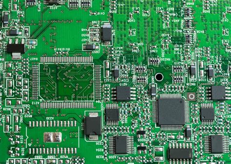
Introduction to Digital PCBs
A printed circuit board (PCB) is the foundation of virtually all modern electronic devices. It mechanically supports and electrically connects electronic components using conductive tracks, pads and other features etched from one or more sheet layers of copper laminated onto and/or between sheet layers of a non-conductive substrate. Digital PCBs are a specific type of PCB designed to transmit digital signals between components.
Digital signals consist of discrete voltage levels representing 1s and 0s — the binary language that computers understand. A digital PCB provides the circuitry to pass these binary signals between chips, processors, memory, and other digital components. The tracks on a digital PCB act as transmission lines, designed with controlled impedance to maintain signal integrity as the square wave pulses travel between devices.
Characteristics of Digital Signals
To understand the unique requirements of digital PCBs, it’s important to first look at the nature of digital signals:
Square Wave Pulses
Digital signals take the form of square wave pulses. Unlike analog signals which are continuously variable, a digital signal can only have two states — high or low, on or off, 1 or 0. The transitions between states are very fast, with rise and fall times measured in nanoseconds.
Clock Signals
Digital systems are synchronized to a master clock which provides regular timing pulses. The clock frequency determines how many pulses (and thus how many bits of data) are transmitted per second. Modern digital devices commonly operate with clock speeds in the gigahertz (GHz) range — billions of cycles per second.
Parallel vs Serial
Digital data can be transmitted in parallel (multiple bits at once over separate lines) or serially (one bit at a time over a single line). Parallel provides higher bandwidth but requires more PCB tracks. Serial is slower but simpler and cheaper to implement. Most digital PCBs use a combination of parallel for internal data buses and serial for external interfaces.

Digital PCB Design Considerations
Designing a high-speed digital PCB presents some unique challenges compared to an analog or low-frequency board. Key factors to consider include:
Controlled Impedance
To maintain signal integrity and minimize reflections, the characteristic impedance of the PCB traces must match the impedance of the driver and receiver circuits (typically 50Ω or 75Ω). This is achieved by carefully controlling the trace width, copper thickness, and dielectric properties of the board material. Impedance calculators are used to determine the required geometry.
Termination
Digital signal lines may need to be terminated with a resistor to prevent reflections. The termination resistor, placed near the receiver end, matches the trace impedance to minimize the reflected energy. Series, parallel, RC, and diode termination schemes are used depending on the application.
Crosstalk
When digital signals transition, the fast edges can capacitively couple to nearby traces causing crosstalk — unwanted noise that can lead to data errors. To minimize crosstalk, sensitive traces are spaced apart or isolated with ground traces, power planes are added for shielding, and dielectric layers are made thinner to reduce coupling.
EMI/EMC
The sharp edges of high-speed digital pulses have significant high-frequency harmonics which can radiate electromagnetic interference (EMI) and cause problems with electromagnetic compatibility (EMC). To mitigate EMI, digital PCBs often include shielding, filtering, and careful layer stackup design to control return currents.
Length Matching
In high-speed parallel interfaces, it’s critical that the propagation delay is equal on all data lines. If one bit arrives before the others, the receiver can latch incorrect data. To avoid this, the trace lengths must be “length matched” so all signals arrive simultaneously. Serpentine routing is often used to add delay to shorter traces.
Decoupling
Digital ICs draw sharp spikes of current from the power supply with every clock cycle. If the power distribution network (PDN) is not low impedance, these spikes can cause the supply voltage to dip, leading to signal integrity issues. Adding decoupling capacitors close to each digital IC stabilizes the supply voltage and shunts high-frequency noise.

Digital PCB Stackup and Layout
The arrangement of copper and insulating layers in a digital PCB — known as the stackup — is critical to its performance. A typical 4-layer digital PCB stackup consists of:
| Layer | Purpose |
|---|---|
| Top | Signals, components |
| Ground plane | Shielding, current return |
| Power plane | Power distribution |
| Bottom | Signals, components |
Additional layers can be added for more complex designs. Sensitive signals are often routed between the planes for maximum shielding.
When laying out a digital PCB, best practices include:
- Route high-speed signals first, on top/bottom layers
- Keep high-speed traces short and direct
- Avoid crossing split planes with signals
- Provide ground stitching vias near connectors
- Use 45° angles instead of 90° corners
- Flood all unused areas with ground fill
- Place decoupling caps close to ICs
- Avoid daisy-chaining vias and connectors
Simulation software is often used to analyze signal integrity before fabrication. Time-domain reflectometry (TDR) can pinpoint discontinuities in a digital PCB design.

Digital PCB Materials
The choice of PCB materials is important for high-speed digital applications. Key parameters include:
Dielectric Constant (Dk)
The dielectric constant of the insulating material between copper layers impacts the trace impedance and propagation velocity. Lower Dk allows thinner boards and faster signals. Common high-speed materials include Rogers, Isola, and Taconic.
Dissipation Factor (Df)
The dissipation factor is a measure of a material’s loss tangent at high frequencies. Higher Df means more signal attenuation. Low-loss materials are essential for multi-gigabit designs.
Coefficient of Thermal Expansion (CTE)
The CTE quantifies how much a material expands with temperature. Mismatches between the CTE of the PCB, copper, components, and solder can lead to mechanical stress and reliability issues. Low-CTE materials are preferred for digital designs.
Digital PCB Testing and Validation
After fabrication, a digital PCB must be thoroughly tested before assembly to ensure signal integrity and catch any manufacturing defects. Common tests include:
- Continuity test – verifies all connections
- Isolation test – checks for shorts between nets
- Impedance test – measures trace impedance
- TDR test – finds impedance discontinuities
- Microsection – cross-section analysis of vias and traces
- Hi-pot test – checks dielectric strength at high voltage
Functional testing with high-speed digital scopes, BERTs (bit error rate testers), and network analyzers is also critical to validate performance at speed. Issues like jitter, eye closure, s-parameters, and EMI are characterized.
Digital PCB Manufacturing Advances
As digital speeds continue to climb, new PCB manufacturing technologies are emerging to keep pace:
HDI (High Density Interconnect)
HDI uses micro vias and fine pitch traces to pack more functionality into a smaller space. Sequential lamination builds up the layers with multiple drill and plating steps. Any-layer HDI allows vias to start and stop on any layer.
VeCS (Very High Density Cable Solution)
VeCS is a proprietary IBM technology that routes signals through ultra-thin cables embedded within the PCB stackup. This allows extremely dense routing of high-speed differential pairs with lower loss and crosstalk than traditional traces.
3D Printing
Inkjet and stereolithography 3D printers can now create PCBs by depositing conductive and insulating inks. This allows more intricate geometries and faster prototyping than conventional etching. The resolution and performance are still limited for high-speed digital but are rapidly improving.
The Future of Digital PCBs
As our world becomes ever more digitally connected, the demand for faster, smaller, cheaper, and more complex digital PCBs will only accelerate. Some key trends shaping the future include:
- Higher speeds – 112G PAM4 and beyond
- Denser packaging – chiplets, 3D ICs
- New materials – graphene, carbon nanotubes
- More layers – 50+ layer stackups
- Rigid-flex – conformable designs
- Embedded components – actives and passives in substrate
- Optical interconnects – fiber and waveguides for Tbps
- Additive manufacturing – 3D printed electronics
- AI-assisted design – automated optimization
- Environmental – green initiatives, recycling
Whatever the future holds, it’s a sure bet that digital PCBs will be at the heart of it, continuing to expand the boundaries of performance, efficiency, and innovation. The humble circuit board has already revolutionized our society, and its potential is still being unlocked. Each new generation of digital PCBs enables a new wave of electronic possibilities.
FAQ
Q1: What is the difference between a digital PCB and an analog PCB?
A1: A digital PCB is specifically designed to carry high-speed digital signals (square waves) between logic devices, whereas an analog PCB handles continuously variable signals like audio and power. Digital PCBs have additional requirements like controlled impedance, length matching, and EMI suppression.
Q2: What is controlled impedance and why is it important for digital PCBs?
A2: Controlled impedance means designing the PCB traces to have a specific characteristic impedance (usually 50Ω or 75Ω) to match the impedance of the driver and receiver. This is critical in high-speed digital PCBs to prevent signal reflections and maintain integrity. The impedance is controlled by the trace geometry and the dielectric constant of the board material.
Q3: How can crosstalk be minimized in a digital PCB design?
A3: Crosstalk is unwanted coupling between adjacent signal traces. It can be minimized by:
- Increasing the spacing between traces
- Adding ground traces or planes between signals
- Using thinner dielectrics to reduce coupling capacitance
- Routing sensitive signals on different layers
- Minimizing parallel run lengths
Q4: What is the purpose of decoupling capacitors in a digital PCB?
A4: Digital ICs draw sharp spikes of current from the power supply with every clock cycle. Decoupling capacitors placed close to each IC help to stabilize the local supply voltage by providing a low-impedance path for these high-frequency transients. This prevents the noise from spreading through the power distribution network and causing signal integrity issues.
Q5: What are some common tests performed on digital PCBs?
A5: Digital PCBs undergo a range of tests to verify signal integrity and catch manufacturing defects:
- Continuity test checks all connections
- Isolation test looks for short circuits
- Impedance test measures trace impedance
- Time-Domain Reflectometry (TDR) finds impedance discontinuities
- Microsection examines via and trace geometry
- High-potential (Hi-pot) test checks dielectric strength
Functional tests are also critical, using high-speed scopes, bit error rate testers (BERTs), and network analyzers to characterize performance at speed. Parameters like jitter, eye diagrams, s-parameters, and EMI are measured.


Leave a Reply