Understanding the PCB Manufacturing Process
The PCB manufacturing process consists of several key stages, each of which plays a crucial role in determining the quality of the final product. These stages include:
- PCB Design
- PCB Fabrication
- PCB Assembly
- PCB Testing and Inspection
PCB Design
The PCB design stage is where the layout and schematic of the board are created using specialized software. Some key considerations during this stage include:
- Component placement
- Signal integrity
- Power distribution
- Thermal management
- Design for manufacturability (DFM)
To ensure optimal PCB design, designers should follow best practices such as:
- Minimizing the number of layers
- Using appropriate trace widths and spacing
- Avoiding sharp angles and using smooth curves
- Incorporating proper grounding and shielding techniques
- Conducting design reviews and simulations
PCB Fabrication
Once the PCB design is finalized, the fabrication process begins. This stage involves several sub-processes, including:
- Substrate preparation
- Copper cladding
- Photoresist application
- Exposure and development
- Etching
- Hole drilling
- Solder mask application
- Silkscreen printing
- Surface finish application
To improve the quality of PCB fabrication, manufacturers should:
- Use high-quality materials and substrates
- Maintain strict process control and monitoring
- Implement automated systems for consistency and accuracy
- Adhere to industry standards and regulations
- Conduct regular maintenance and calibration of equipment
PCB Assembly
PCB assembly involves the placement and soldering of components onto the fabricated board. The two main methods of PCB assembly are:
- Through-hole assembly (THA)
- Surface mount assembly (SMA)
To optimize the PCB assembly process, consider the following:
- Use automated pick-and-place machines for precise component placement
- Implement solder paste inspection (SPI) to ensure proper solder paste application
- Utilize appropriate soldering techniques (e.g., wave soldering, reflow soldering)
- Conduct post-assembly cleaning to remove flux residue and contaminants
- Perform visual inspections and automated optical inspection (AOI) to detect defects
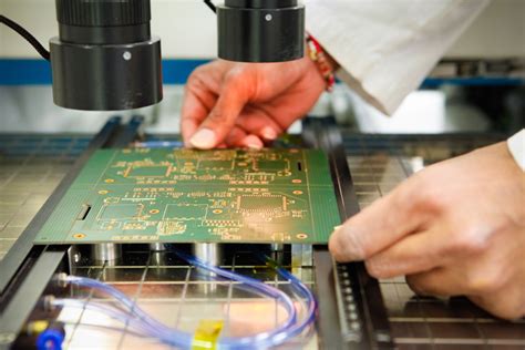
PCB Testing and Inspection
Thorough testing and inspection are essential to ensure the quality and reliability of the manufactured PCBs. Some common testing and inspection methods include:
- In-circuit testing (ICT)
- Functional testing
- Boundary scan testing
- X-ray inspection
- Thermal imaging
To improve PCB testing and inspection, manufacturers should:
- Develop comprehensive test plans and procedures
- Use advanced testing equipment and software
- Implement statistical process control (SPC) to monitor and analyze test results
- Conduct root cause analysis and implement corrective actions for identified issues
- Maintain detailed documentation and traceability records
Choosing the Right PCB Manufacturer
Selecting a reliable and experienced PCB manufacturer is crucial for ensuring the quality and success of your PCB project. When evaluating potential manufacturers, consider the following factors:
- Manufacturing capabilities and capacity
- Quality control processes and certifications (e.g., ISO 9001, IPC standards)
- Technical expertise and support
- Turnaround time and delivery performance
- Pricing and cost-effectiveness
- Customer reviews and references
To help you make an informed decision, here’s a comparison table of key factors for three hypothetical PCB manufacturers:
| Factor | Manufacturer A | Manufacturer B | Manufacturer C |
|---|---|---|---|
| Manufacturing Capacity | High | Medium | Low |
| Quality Certifications | ISO 9001, IPC | ISO 9001 | IPC |
| Technical Support | Excellent | Good | Fair |
| Turnaround Time | Fast | Moderate | Slow |
| Pricing | Competitive | Average | Expensive |
| Customer Reviews | Positive | Mixed | Limited |

Optimizing PCB Manufacturing for Specific Applications
Different applications may require specific considerations and optimizations in the PCB manufacturing process. Some common application-specific considerations include:
High-Frequency PCBs
- Use low-loss dielectric materials
- Minimize trace lengths and use controlled impedance routing
- Implement proper grounding and shielding techniques
- Use surface mount components to reduce parasitic inductance
High-Power PCBs
- Use thicker copper layers for improved current carrying capacity
- Implement adequate cooling and thermal management techniques
- Use appropriate component ratings and power handling capabilities
- Consider using metal core PCBs (MCPCBs) for enhanced thermal dissipation
Flexible PCBs
- Choose appropriate flexible substrate materials (e.g., polyimide, PET)
- Use thin copper layers to maintain flexibility
- Implement strain relief features and reinforced areas for connector attachment
- Consider the bending radius and flexing requirements during design and manufacturing
Automotive and Aerospace PCBs
- Adhere to industry-specific standards and regulations (e.g., AEC-Q100, DO-160)
- Use high-reliability components and materials
- Implement robust testing and qualification processes
- Consider environmental factors such as temperature, vibration, and humidity

Frequently Asked Questions (FAQ)
-
Q: What is the difference between through-hole and surface mount assembly?
A: Through-hole assembly involves inserting component leads through drilled holes in the PCB and soldering them on the opposite side. Surface mount assembly involves placing components directly onto the PCB surface and soldering them using reflow or wave soldering techniques. -
Q: What are the main factors affecting PCB Manufacturing Costs?
A: PCB manufacturing costs are influenced by several factors, including board size, layer count, material selection, component density, manufacturing volume, and turnaround time. More complex and higher-volume projects generally result in lower per-unit costs. -
Q: How can I ensure my PCB design is manufacturable?
A: To ensure your PCB design is manufacturable, follow design for manufacturability (DFM) guidelines, such as using appropriate trace widths and spacing, minimizing the number of layers, avoiding sharp angles, and incorporating proper grounding and shielding techniques. Consult with your PCB manufacturer early in the design process for specific DFM recommendations. -
Q: What are the most common PCB Manufacturing Defects?
A: Common PCB manufacturing defects include solder bridging, cold solder joints, tombstoning, component misalignment, insufficient solder, and lifted pads. These defects can be minimized through proper process control, automated inspection, and adherence to best practices in design and manufacturing. -
Q: How long does it typically take to manufacture a PCB?
A: The lead time for PCB manufacturing varies depending on the complexity of the design, the manufacturing processes involved, and the workload of the manufacturer. Typical lead times range from a few days to several weeks. Expedited services may be available for faster turnaround times, but they often come at a higher cost.

Conclusion
Printed Circuit Board (PCB) manufacturing is a complex process that requires careful consideration and optimization at every stage to ensure the production of high-quality boards. By understanding the key aspects of PCB design, fabrication, assembly, and testing, and by implementing best practices and application-specific optimizations, you can significantly improve the quality and reliability of your PCBs.
When selecting a PCB manufacturer, it is essential to evaluate their capabilities, quality control processes, technical expertise, and customer support to ensure they can meet your specific requirements. By partnering with a reputable and experienced manufacturer and following the guidelines outlined in this article, you can successfully navigate the PCB manufacturing process and achieve better results for your projects.


Leave a Reply