Table of Contents
- Introduction to Op-Amps
- LM358 Key Features and Specifications
- Pinout and Package Options
- Circuit Configuration and Applications
- Voltage Follower
- Inverting Amplifier
- Non-Inverting Amplifier
- Summing Amplifier
- Differential Amplifier
- Comparator
- Oscillators and Waveform Generators
- Active Filters
- Practical Considerations
- Input and Output Voltage Range
- Input Bias Current
- Offset Voltage
- Slew Rate
- Noise
- Example Projects
- Temperature Sensor with LM358
- Audio Preamplifier using LM358
- PWM Motor Speed Control with LM358
- Frequently Asked Questions (FAQ)
- Conclusion
Introduction to Op-Amps
An operational amplifier, or op-amp, is a high-gain electronic voltage amplifier with differential inputs and a single output. Op-amps are designed to perform mathematical operations like amplification, attenuation, addition, subtraction, integration, and differentiation on analog signals.
The ideal op-amp has the following characteristics:
– Infinite open-loop gain
– Infinite input impedance
– Zero output impedance
– Infinite bandwidth
– Zero input offset voltage
– Zero noise
While real op-amps cannot achieve these ideal characteristics, they come close enough for most practical applications. Op-amps are commonly used in analog circuits for signal conditioning, filtering, buffering, and mathematical operations.

LM358 Key Features and Specifications
The LM358 is a dual op-amp IC that offers the following key features:
- Low supply current drain (500 μA per amplifier)
- Wide power supply voltage range (3V to 32V for single supply, ±1.5V to ±16V for dual supplies)
- Low input bias current (−45 nA to −250 nA)
- Low input offset voltage (2 mV to 7 mV)
- High gain bandwidth product (1 MHz)
- High slew rate (0.3 V/μs to 0.7 V/μs)
- Input common-mode voltage range includes ground
- Differential input voltage range equal to the power supply voltage
- Internal frequency compensation
The table below summarizes the key specifications of the LM358 op-amp:
| Parameter | Min | Typ | Max | Units |
|---|---|---|---|---|
| Supply Voltage (VS) | 3 | – | 32 | V |
| Supply Current (IS) | – | 0.5 | 1.2 | mA |
| Input Offset Voltage (VIO) | – | 2 | 7 | mV |
| Input Bias Current (IB) | -45 | -100 | -250 | nA |
| Input Impedance (Zin) | – | 1 | – | TΩ |
| Output Voltage Swing (VO) | 0 | – | VS-1.5 | V |
| Gain Bandwidth Product (GBP) | – | 1 | – | MHz |
| Slew Rate (SR) | 0.3 | 0.5 | 0.7 | V/μs |
| Operating Temperature Range | -40 | – | 85 | °C |

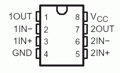
Pinout and Package Options
The LM358 is available in several package options, including 8-pin DIP (Dual Inline Package), SOIC (Small Outline Integrated Circuit), and TSSOP (Thin-Shrink Small Outline Package). The pinout for the 8-pin DIP package is shown below:
      +-------+
  OUT 1 |1   8| V+
  IN- 1 |2   7| OUT 2
  IN+ 1 |3   6| IN- 2
  GND   |4   5| IN+ 2
      +-------+
- Pin 1: Output of op-amp 1
- Pin 2: Inverting input of op-amp 1
- Pin 3: Non-inverting input of op-amp 1
- Pin 4: Ground (0 V)
- Pin 5: Non-inverting input of op-amp 2
- Pin 6: Inverting input of op-amp 2
- Pin 7: Output of op-amp 2
- Pin 8: Positive supply voltage (V+)
Note that the two op-amps share the same power supply pins (V+ and GND) but have separate inputs and outputs.

Circuit Configuration and Applications
The LM358 can be used in various circuit configurations to perform different functions. Let’s explore some common applications and their corresponding circuit diagrams.
Voltage Follower
A voltage follower, also known as a unity gain buffer, is used to isolate a high-impedance source from a low-impedance load. The output voltage follows the input voltage, providing a low-impedance output that can drive heavier loads without affecting the input signal.
             +--[R1]--+
   VIN ------|+       |
             |    OUT |------> VOUT
             |-       |
             |        |
             +--------+
                 GND
The gain of a voltage follower is 1, meaning the output voltage equals the input voltage.
Inverting Amplifier
An inverting amplifier multiplies the input signal by a constant factor (gain) and inverts its polarity. The gain is determined by the ratio of the feedback resistor (R2) to the input resistor (R1).
                  +--[R2]--+
                  |        |
   VIN ---[R1]----|-       |
                  |    OUT |------> VOUT
                  |+       |
                  |        |
                  +--------+
                      GND
The gain of an inverting amplifier is given by:
Gain = -R2 / R1
For example, if R1 = 1 kΩ and R2 = 10 kΩ, the gain would be -10.
Non-Inverting Amplifier
A non-inverting amplifier multiplies the input signal by a constant factor without inverting its polarity. The gain is determined by the ratio of the feedback resistor (R2) to the input resistor (R1).
             +--[R1]--+
             |        |
   VIN ------|+       |
             |        |
             |   [R2] |
             |        |
             |-       |
             |    OUT |------> VOUT
             |        |
             +--------+
                 GND
The gain of a non-inverting amplifier is given by:
Gain = 1 + (R2 / R1)
For example, if R1 = 1 kΩ and R2 = 9 kΩ, the gain would be 10.
Summing Amplifier
A summing amplifier adds multiple input signals together, with each input having its own gain determined by the ratio of the feedback resistor (Rf) to the input resistor (R1, R2, etc.).
                 +--[Rf]--+
                 |        |
   VIN1 --[R1]---|-       |
                 |        |
   VIN2 --[R2]---|-       |
                 |    OUT |------> VOUT
   VIN3 --[R3]---|-       |
                 |        |
                 |+       |
                 |        |
                 +--------+
                     GND
The output voltage is given by:
VOUT = -(Rf/R1 × VIN1 + Rf/R2 × VIN2 + Rf/R3 × VIN3)
Differential Amplifier
A differential amplifier amplifies the difference between two input signals while rejecting common-mode signals. The gain is determined by the ratio of the feedback resistors (R2 and R4) to the input resistors (R1 and R3).
                +--[R2]--+
                |        |
   VIN+ --[R1]--|-       |
                |    OUT |------> VOUT
   VIN- --[R3]--|+       |
                |        |
                +--[R4]--+
                    GND
The output voltage is given by:
VOUT = (R4/R3) × [(R2/R1 + 1) × VIN+ - VIN-]
For best performance, use matched resistors such that R2/R1 = R4/R3.
Comparator
A comparator compares two input voltages and produces a digital output indicating which input is higher. The LM358 can be used as a comparator by leaving the feedback resistor unconnected.
             +
   VIN+ ------|+
             |
   VIN- ------|−
             |    OUT |------> VOUT
             |        |
             +--------+
                 GND
When VIN+ > VIN-, the output will be high (close to V+). When VIN- > VIN+, the output will be low (close to GND).
Oscillators and Waveform Generators
The LM358 can be used to create various oscillators and waveform generators by incorporating feedback networks with specific frequency-determining components like resistors and capacitors. Examples include:
- Astable multivibrator (square wave generator)
- Schmitt trigger
- Wien bridge oscillator (sine wave generator)
- Triangle wave generator
Active Filters
Active filters use op-amps in combination with passive components (resistors and capacitors) to implement frequency-selective circuits. The LM358 can be used to build various filter topologies, such as:
- Low-pass filter
- High-pass filter
- Band-pass filter
- Band-stop (notch) filter
Practical Considerations
When using the LM358 op-amp in real-world applications, there are several practical considerations to keep in mind:
Input and Output Voltage Range
The input voltage range of the LM358 extends from the negative supply voltage (GND) to approximately 1.5 V below the positive supply voltage (V+). The output voltage swing is also limited by the supply voltages, typically reaching within 1.5 V of either supply rail.
Input Bias Current
The LM358 has a relatively high input bias current (up to -250 nA), which can cause voltage drops across high-value resistors. This effect can be minimized by using lower-value resistors or by compensating for the bias current using a resistor in series with the non-inverting input.
Offset Voltage
The input offset voltage of the LM358 can vary from 2 mV to 7 mV, which may cause errors in high-precision applications. Offset voltage can be minimized by using a potentiometer to adjust the balance between the inputs or by using an auto-zero technique.
Slew Rate
The slew rate of the LM358 is relatively low (0.3 V/μs to 0.7 V/μs), which limits its ability to handle high-frequency signals without distortion. This should be considered when using the LM358 in applications that require fast signal transitions.
Noise
The LM358 has a moderate level of noise, which can be a concern in low-signal applications. Noise can be minimized by using proper circuit layout techniques, such as keeping signal traces short, using ground planes, and bypassing power supply pins with capacitors.
Example Projects
Here are a few example projects that demonstrate the use of the LM358 op-amp in practical applications:
Temperature Sensor with LM358
A temperature sensor, such as the LM35, can be interfaced with an LM358 to create a temperature monitoring system. The LM358 amplifies the sensor’s output voltage and provides a scaled output that can be read by an ADC or microcontroller.
Audio Preamplifier using LM358
The LM358 can be used to build a simple audio preamplifier for microphones or other low-level audio sources. The preamplifier provides gain and impedance matching to drive subsequent stages, such as power amplifiers or ADCs.
PWM Motor Speed Control with LM358
An LM358 can be used to implement a PWM (Pulse Width Modulation) motor speed control circuit. The op-amp compares a reference voltage with a sawtooth waveform to generate a PWM signal that controls the motor speed via a power transistor or H-bridge.
Frequently Asked Questions (FAQ)
-
Can the LM358 be used with a single power supply?
Yes, the LM358 is designed to operate with a single power supply ranging from 3 V to 32 V. The input and output voltages are referenced to the negative supply pin (GND). -
Is the LM358 suitable for audio applications?
The LM358 can be used in audio applications, such as preamplifiers and tone controls. However, its relatively low slew rate and moderate noise performance may limit its use in high-fidelity or professional audio systems. -
Can the LM358 be used as a comparator?
Yes, the LM358 can be used as a comparator by leaving the feedback resistor unconnected. When configured as a comparator, the output will swing between the positive and negative supply voltages based on the relative levels of the input signals. -
How do I minimize the effect of input bias current in LM358 circuits?
To minimize the effect of input bias current, use lower-value resistors in the feedback network or compensate for the bias current by adding a resistor in series with the non-inverting input, equal in value to the parallel combination of the resistors connected to the inverting input. -
What is the maximum supply voltage for the LM358?
The maximum supply voltage for the LM358 is 32 V for single-supply operation and ±16 V for dual-supply operation. Always consult the manufacturer’s datasheet for the most up-to-date specifications.
Conclusion
The LM358 op-amp is a versatile and cost-effective choice for a wide range of analog applications. Its key features, such as low power consumption, wide supply voltage range, and good performance characteristics, make it suitable for use in signal conditioning, amplification, filtering, and comparator circuits.
By understanding the LM358’s specifications, circuit configurations, and practical considerations, designers can effectively integrate this op-amp into their projects. Whether building a temperature sensor, audio preamplifier, or PWM motor speed control, the LM358 provides a reliable and affordable solution.
As with any electronic component, it is essential to consult the manufacturer’s datasheet and application notes for the most accurate and up-to-date information. Additionally, proper circuit layout techniques and testing should be employed to ensure optimal performance and reliability in the final application.


Leave a Reply