Introduction to PCB Trace Repair
Printed Circuit Boards (PCBs) are essential components in modern electronics, connecting various components to create functional devices. However, PCBs can suffer from damage, such as broken or corroded traces, which can lead to malfunctions or complete failure of the device. PCB trace repair is a crucial skill for anyone working with electronics, as it can save time and money by fixing damaged boards instead of replacing them entirely.
In this article, we will explore the process of PCB trace repair, including the tools and techniques required to successfully repair damaged traces. We will also discuss the importance of proper safety measures and the benefits of using a PCB trace repair kit.
What is a PCB Trace?
A PCB trace is a conductive pathway that connects components on a printed circuit board. These traces are typically made of copper and are etched onto the board during the manufacturing process. They allow electrical signals to flow between components, enabling the device to function as intended.
PCB traces come in various widths and thicknesses, depending on the current requirements and the overall design of the board. They can be found on both sides of a PCB, with connections between layers made through vias (small holes filled with conductive material).

Common Causes of PCB Trace Damage
PCB traces can become damaged due to several reasons, including:
- Physical damage: Accidental impacts, drops, or improper handling can cause traces to crack or break.
- Overheating: Excessive heat, often caused by overcurrent or poor ventilation, can lead to trace damage or delamination.
- Corrosion: Exposure to moisture, chemicals, or other corrosive agents can cause traces to deteriorate over time.
- Manufacturing defects: Imperfections during the PCB manufacturing process, such as incorrect etching or poor quality control, can result in trace damage.

Tools Required for PCB Trace Repair
To effectively repair damaged PCB traces, you will need the following tools:
- Soldering iron: A temperature-controlled soldering iron with a fine tip is essential for precise trace repair work.
- Solder: Use high-quality, lead-free solder designed for electronics work.
- Flux: Flux helps to clean the surface of the PCB and promotes better solder adhesion.
- Solder wick: Also known as desoldering braid, solder wick is used to remove excess solder from the repair area.
- Copper tape or conductive ink pen: These materials are used to bridge gaps in damaged traces.
- Magnifying glass or microscope: A magnifying tool helps to inspect the damaged area and ensures precise repairs.
- Tweezers: Precision tweezers are useful for handling small components and manipulating copper tape or other repair materials.
- Cleaning supplies: Isopropyl alcohol, cotton swabs, and a soft brush are used to clean the PCB before and after the repair process.

Safety Precautions
Before beginning any PCB trace repair work, it is crucial to take proper safety precautions:
- Work in a well-ventilated area to avoid inhaling fumes from soldering or cleaning agents.
- Wear protective eyewear to shield your eyes from debris or splashes.
- Use a grounded soldering iron and work on an ESD-safe surface to prevent electrostatic discharge damage to the PCB or components.
- Allow the soldering iron and repaired PCB to cool completely before handling or storing.
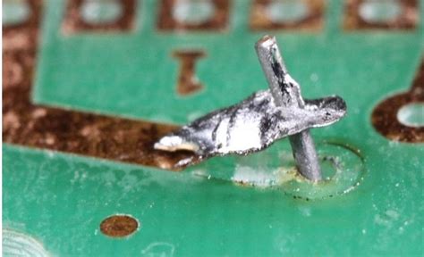
Step-by-Step Guide to PCB Trace Repair
Step 1: Identify the Damaged Trace
Use a magnifying glass or microscope to carefully inspect the PCB and locate the damaged trace. Look for cracks, breaks, or signs of corrosion.
Step 2: Clean the Repair Area
Clean the area around the damaged trace using isopropyl alcohol and a cotton swab or soft brush. This removes any dirt, grease, or oxidation that may interfere with the repair process.
Step 3: Remove Damaged Trace Material
If there is any loose or damaged trace material, carefully remove it using tweezers or a scalpel. Be cautious not to damage surrounding components or traces.
Step 4: Apply Flux
Apply a small amount of flux to the repair area. This will help the solder to flow smoothly and adhere to the PCB surface.
Step 5: Bridge the Gap
Using copper tape or a conductive ink pen, carefully bridge the gap in the damaged trace. Ensure that the new connection is securely attached to the existing trace on both sides of the break.
Step 6: Solder the Repair
Heat the soldering iron and apply a small amount of solder to the tip. Gently touch the iron to the repair area, allowing the solder to flow over the copper tape or conductive ink. Be careful not to apply too much heat, as this can cause further damage to the PCB.
Step 7: Remove Excess Solder
If necessary, use solder wick to remove any excess solder from the repair area. Place the wick over the excess solder and heat it with the soldering iron. The solder will be drawn up into the wick, leaving a clean and tidy repair.
Step 8: Clean and Inspect
Clean the repaired area once more with isopropyl alcohol and inspect the work using a magnifying glass or microscope. Ensure that the new connection is secure and that there is no excess solder bridging other traces or components.
Benefits of Using a PCB Trace Repair Kit
A PCB trace repair kit is a convenient and cost-effective solution for anyone who frequently works with PCBs. These kits typically include all the necessary tools and materials for trace repair, such as:
- Soldering iron and solder
- Flux and solder wick
- Copper tape or conductive ink pen
- Tweezers and magnifying glass
- Cleaning supplies
By investing in a PCB trace repair kit, you can save time and money by having all the essential tools readily available when needed. This eliminates the need to purchase items separately and ensures that you have the right tools for the job.
Alternatives to PCB Trace Repair
In some cases, PCB trace repair may not be the most suitable option. Alternative solutions include:
- Bodge wires: Bodge wires are insulated wires that can be used to bypass damaged traces. They are soldered directly to the component leads, creating a new connection path.
- Jumper wires: Similar to bodge wires, jumper wires can be used to bridge damaged traces. They are typically used for shorter distances and are soldered to the PCB surface.
- PCB replacement: If the damage to the PCB is extensive or if the board is particularly valuable, it may be more cost-effective to replace the entire PCB rather than attempt a repair.
Frequently Asked Questions (FAQ)
1. Can I use regular solder for PCB trace repair?
While it is possible to use regular solder for PCB trace repair, it is recommended to use lead-free solder specifically designed for electronics work. Lead-free solder has a higher melting point and provides a stronger, more reliable connection.
2. How do I prevent PCB trace damage?
To prevent PCB trace damage, handle boards with care, avoid exposing them to excessive heat or moisture, and ensure proper storage when not in use. Additionally, use appropriate ESD protection measures when working with PCBs to prevent electrostatic discharge damage.
3. Can I repair a PCB trace without a soldering iron?
While it is possible to use conductive adhesives or other alternative methods for PCB trace repair, using a soldering iron is the most reliable and durable approach. Soldering ensures a strong, conductive connection that will withstand the test of time.
4. How long does a PCB trace repair typically take?
The time required for a PCB trace repair depends on the extent of the damage and the complexity of the repair. Simple repairs can be completed in a matter of minutes, while more intricate work may take several hours.
5. Is it safe to use a PCB trace repair kit at home?
Yes, it is safe to use a PCB trace repair kit at home, provided that you follow proper safety precautions. Work in a well-ventilated area, wear protective eyewear, and use a grounded soldering iron to prevent electrostatic discharge damage.
Conclusion
PCB trace repair is an essential skill for anyone working with electronics. By mastering the tools and techniques required for successful trace repair, you can save time, money, and resources by fixing damaged boards instead of replacing them entirely. A PCB trace repair kit is a valuable investment for anyone who frequently works with PCBs, providing all the necessary tools and materials in one convenient package.
Remember to always prioritize safety when working with PCBs, and take the time to carefully inspect and clean the repair area before beginning any work. With practice and patience, anyone can become proficient in PCB trace repair and enjoy the benefits of this valuable skill.
| Tool | Purpose |
|---|---|
| Soldering iron | Used for melting solder and creating conductive connections |
| Solder | A metal alloy used to create conductive connections |
| Flux | Helps to clean the PCB surface and promote solder adhesion |
| Solder wick | Used to remove excess solder from the repair area |
| Copper tape or conductive ink pen | Used to bridge gaps in damaged traces |
| Magnifying glass or microscope | Helps to inspect the damaged area and ensure precise repairs |
| Tweezers | Useful for handling small components and manipulating repair materials |
| Cleaning supplies | Used to clean the PCB before and after the repair process |


Leave a Reply