Introduction to BJT Load Line
In the world of electronics, understanding the behavior of transistors is crucial for designing and analyzing circuits. One of the most commonly used transistors is the Bipolar Junction Transistor (BJT). To properly analyze and design circuits using BJTs, it’s essential to understand the concept of the load line. In this article, we will dive deep into the BJT load line, its characteristics, and how it helps in understanding the function of BJTs in various circuit configurations.
What is a BJT?
Before we delve into the load line, let’s briefly review what a BJT is. A BJT is a three-terminal semiconductor device that consists of two types of semiconductors, namely, the emitter, base, and collector. BJTs come in two flavors: NPN and PNP, depending on the arrangement of the semiconductor materials. BJTs are widely used in amplifiers, switches, and other electronic circuits due to their ability to control large currents with small input signals.
The Concept of Load Line
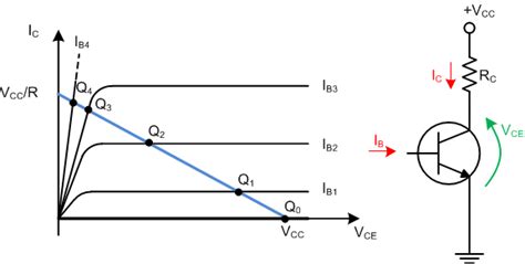
The load line is a graphical representation of the relationship between the collector current (IC) and the collector-emitter voltage (VCE) of a BJT in a particular circuit configuration. It helps in determining the operating point, also known as the quiescent point (Q-point), of the transistor. The load line is drawn on the BJT’s characteristic curves, which show the relationship between IC and VCE for different values of base current (IB).
Constructing the Load Line
To construct the load line, we need to consider the circuit in which the BJT is connected. Let’s take a common emitter configuration as an example, where the emitter is grounded, and the collector is connected to the positive supply voltage (VCC) through a resistor (RC).
Step 1: Determine the Saturation Current (IC(sat))
The saturation current is the maximum collector current that can flow when the transistor is fully on (saturated). It is determined by the supply voltage and the collector resistor value:
IC(sat) = VCC / RC
For example, if VCC = 10V and RC = 1kΩ, then IC(sat) = 10mA.
Step 2: Determine the Cutoff Voltage (VCE(cutoff))
The cutoff voltage is the maximum collector-emitter voltage when the transistor is fully off (cutoff). In this case, it is equal to the supply voltage:
VCE(cutoff) = VCC
In our example, VCE(cutoff) = 10V.
Step 3: Plot the Load Line
On the BJT characteristic curves, locate the points corresponding to IC(sat) on the vertical axis and VCE(cutoff) on the horizontal axis. Draw a straight line connecting these two points. This line represents the load line for the given circuit configuration.

Analyzing the Load Line
Once the load line is constructed, we can use it to analyze the behavior of the BJT in the circuit. Let’s look at some key points and regions on the load line.
Quiescent Point (Q-Point)
The quiescent point, or Q-point, is the operating point of the transistor when no input signal is applied. It is determined by the intersection of the load line with the appropriate base current curve (IB). The Q-point provides information about the collector current and collector-emitter voltage under steady-state conditions.
Active Region
The active region is the portion of the load line where the BJT operates as an amplifier. In this region, the collector current is proportional to the base current, and the transistor exhibits a high output resistance. The active region lies between the saturation and cutoff regions on the load line.
Saturation Region
The saturation region is the portion of the load line where the transistor is fully on, and the collector current is at its maximum value (IC(sat)). In this region, the collector-emitter voltage is close to zero, and the transistor acts like a closed switch.
Cutoff Region
The cutoff region is the portion of the load line where the transistor is fully off, and the collector current is zero. In this region, the collector-emitter voltage is at its maximum value (VCE(cutoff)), and the transistor acts like an open switch.

Load Line in Different Circuit Configurations
The load line concept can be applied to various BJT circuit configurations, such as common emitter, common collector, and common base. Each configuration has its own set of characteristics and load line equations.
Common Emitter Configuration
In the common emitter configuration, the emitter is grounded, and the collector is connected to the supply voltage through a resistor. The load line equation for this configuration is:
IC = (VCC – VCE) / RC
Common Collector Configuration
In the common collector configuration, also known as the emitter follower, the collector is connected to the supply voltage, and the emitter is connected to the load resistor. The load line equation for this configuration is:
IE = (VCC – VE) / (RE + Rload)
Common Base Configuration
In the common base configuration, the base is grounded, and the emitter is the input terminal. The load line equation for this configuration is:
IC = (VCC – VCB) / RC

Load Line and Biasing
The load line is also useful in determining the proper biasing of a BJT circuit. Biasing refers to the process of setting the Q-point of the transistor to ensure that it operates in the desired region (usually the active region) for the intended application.
Fixed Bias
In a fixed bias configuration, the base voltage is set using a voltage divider network. The Q-point is determined by the intersection of the load line with the base current curve corresponding to the fixed base voltage.
Emitter Bias
In an emitter bias configuration, a resistor is connected between the emitter and ground, which provides negative feedback and helps stabilize the Q-point against variations in temperature and transistor parameters.
Load Line and AC Analysis
While the load line is primarily used for DC analysis, it can also provide insights into the AC behavior of the BJT circuit. The AC load line is a graphical representation of the relationship between the AC collector current (ic) and the AC collector-emitter voltage (vce) when an AC input signal is applied.
AC Load Line Equation
The AC load line equation is similar to the DC load line equation, but it takes into account the AC collector resistance (rc) and the AC load resistance (RL):
ic = -vce / (rc + RL)
The slope of the AC load line is determined by the parallel combination of rc and RL.
AC Gain
The AC gain of the BJT circuit can be determined from the AC load line. It is the ratio of the AC output voltage to the AC input voltage. The AC gain is influenced by the slope of the AC load line and the position of the Q-point on the DC load line.
Conclusion
The BJT load line is a powerful tool for analyzing and designing BJT circuits. It provides a graphical representation of the relationship between the collector current and collector-emitter voltage, allowing engineers to determine the operating point, regions of operation, and biasing conditions of the transistor. By understanding the load line concept and its applications in various circuit configurations, designers can optimize the performance of BJT-based circuits and ensure reliable operation.
Frequently Asked Questions (FAQ)
-
What is a BJT load line?
A BJT load line is a graphical representation of the relationship between the collector current and collector-emitter voltage of a BJT in a particular circuit configuration. It helps in determining the operating point and regions of operation of the transistor. -
How is the load line constructed?
The load line is constructed by plotting two points on the BJT characteristic curves: the saturation current point (IC(sat)) on the vertical axis and the cutoff voltage point (VCE(cutoff)) on the horizontal axis. A straight line is then drawn connecting these two points, representing the load line for the given circuit configuration. -
What is the Q-point, and how is it determined using the load line?
The Q-point, or quiescent point, is the operating point of the transistor when no input signal is applied. It is determined by the intersection of the load line with the appropriate base current curve (IB) on the BJT characteristic curves. -
What are the different regions of operation on the load line?
The load line is divided into three regions of operation: the active region, where the BJT operates as an amplifier; the saturation region, where the transistor is fully on; and the cutoff region, where the transistor is fully off. -
How does the load line help in biasing a BJT circuit?
The load line helps in determining the proper biasing of a BJT circuit by setting the Q-point in the desired region of operation (usually the active region). Different biasing techniques, such as fixed bias and emitter bias, can be analyzed using the load line to ensure stable operation of the transistor.
| Parameter | Description |
|---|---|
| IC(sat) | Saturation current, the maximum collector current when the transistor is fully on |
| VCE(cutoff) | Cutoff voltage, the maximum collector-emitter voltage when the transistor is fully off |
| IC | Collector current |
| VCE | Collector-emitter voltage |
| IB | Base current |
| VCC | Supply voltage |
| RC | Collector resistor |
| RE | Emitter resistor |
| Rload | Load resistor |
| ic | AC collector current |
| vce | AC collector-emitter voltage |
| rc | AC collector resistance |
| RL | AC load resistance |


Leave a Reply