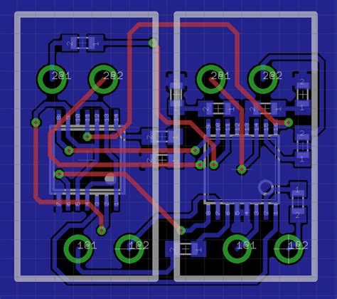
1. Component Placement and Routing
1.1 Optimal Component Arrangement
When placing components on your PCB, it’s crucial to consider their arrangement carefully. Proper component placement can minimize signal interference, reduce the overall size of the board, and improve manufacturability. Here are some tips for optimal component arrangement:
- Group related components together based on their functionality
- Place sensitive components, such as high-speed devices or analog circuits, away from potential sources of noise
- Arrange components in a logical flow, following the signal path from input to output
- Consider the physical dimensions of components and their required clearances
1.2 Efficient Routing Techniques
Once you’ve determined the component placement, the next step is to route the traces that connect them. Efficient routing is essential for maintaining signal integrity and minimizing crosstalk. Keep these techniques in mind:
- Use the shortest possible trace lengths to reduce signal propagation delays and minimize noise pickup
- Avoid sharp angles or corners in traces, as they can cause reflections and degrade signal quality
- Maintain consistent trace widths and spacing, especially for high-speed signals
- Employ appropriate routing strategies, such as daisy-chaining or star topology, based on the specific requirements of your design
| Routing Strategy | Description | Advantages | Disadvantages |
|---|---|---|---|
| Daisy-Chaining | Components are connected in a linear fashion, with the output of one component feeding into the input of the next | Simplifies routing and reduces the number of traces | Increases signal propagation delays and may degrade signal quality |
| Star Topology | Each component is connected directly to a central point, such as a power or ground plane | Minimizes signal propagation delays and reduces noise coupling | Requires more traces and may increase board size |
2. Power Distribution and Grounding
2.1 Proper Power Plane Design
A well-designed power distribution network is essential for providing clean and stable power to all components on your PCB. When designing your power planes, consider the following:
- Use dedicated power planes for each voltage level required by your components
- Ensure adequate copper thickness and width to handle the expected current demands
- Employ appropriate decoupling capacitors near power pins of components to suppress high-frequency noise
- Minimize the impedance of the power distribution network to prevent voltage fluctuations
2.2 Effective Grounding Strategies
Proper grounding is crucial for minimizing noise, preventing ground loops, and ensuring the overall stability of your PCB. Here are some effective grounding strategies:
- Use a solid ground plane to provide a low-impedance return path for signals
- Connect ground pins of components directly to the ground plane using short traces or vias
- Implement a star ground topology for sensitive analog circuits to isolate them from digital noise
- Avoid creating ground loops by ensuring that there is only one path for ground currents to flow

3. Signal Integrity and EMI/EMC Considerations
3.1 Managing Signal Integrity
Maintaining signal integrity is critical for ensuring reliable communication between components on your PCB. To manage signal integrity effectively, keep these points in mind:
- Match the impedance of traces to the characteristic impedance of the components they connect
- Use appropriate termination techniques, such as series or parallel termination, to minimize reflections
- Employ differential signaling for high-speed interfaces to reduce noise and crosstalk
- Avoid crossing signal traces on adjacent layers, as this can lead to unwanted coupling
3.2 Minimizing Electromagnetic Interference (EMI) and Ensuring Electromagnetic Compatibility (EMC)
EMI and EMC are essential considerations in PCB design to prevent interference with other electronic devices and ensure compliance with regulatory standards. Here are some strategies to minimize EMI and ensure EMC:
- Implement proper shielding techniques, such as using ground planes or conductive enclosures, to contain electromagnetic radiation
- Route high-speed signals on inner layers, sandwiched between ground planes, to minimize radiation
- Use appropriate filtering techniques, such as ferrite beads or LC filters, to suppress high-frequency noise
- Ensure proper grounding of connectors and cables to prevent external EMI from entering the system

4. Thermal Management
4.1 Identifying and Addressing Hot Spots
Thermal management is crucial for preventing component overheating and ensuring long-term reliability. To identify and address potential hot spots on your PCB, consider the following:
- Perform thermal simulations or use thermal imaging to identify areas of high heat dissipation
- Place high-power components, such as voltage regulators or power amplifiers, away from temperature-sensitive devices
- Use thermal vias or heat sinks to dissipate heat from components with high thermal output
- Ensure adequate airflow around the PCB to facilitate convective cooling
4.2 Designing for Optimal Heat Dissipation
Proper PCB design can significantly improve heat dissipation and prevent thermal issues. Here are some design techniques to optimize heat dissipation:
- Use wide, thick traces for high-current paths to minimize resistive heating
- Employ copper pours or polygons on unused areas of the PCB to increase thermal conductivity
- Consider using thermal interface materials, such as thermal pads or compounds, to enhance heat transfer between components and the PCB
- Incorporate thermal relief pads around through-hole components to prevent solder joint cracking due to thermal stress

5. Manufacturing Considerations
5.1 Design for Manufacturability (DFM)
Designing your PCB with manufacturability in mind can save time, reduce costs, and improve the overall quality of the final product. Here are some DFM guidelines to follow:
- Adhere to the minimum trace width and spacing specifications provided by your PCB manufacturer
- Ensure proper clearances around components and between copper features to avoid short circuits
- Use standard component sizes and footprints whenever possible to simplify assembly and sourcing
- Avoid using complex or non-standard shapes for copper features, as they may be difficult to manufacture
5.2 Panelization and Tooling
If your design involves multiple identical PCBs, panelization can streamline the manufacturing process and reduce costs. When panelizing your design, keep these points in mind:
- Leave sufficient space between individual boards to accommodate tooling and separation processes
- Incorporate fiducial marks or tooling holes to ensure precise alignment during assembly
- Consider the panel size and aspect ratio to maximize material utilization and minimize waste
- Discuss panelization options and requirements with your PCB manufacturer to ensure compatibility with their processes
6. Documentation and Communication
6.1 Creating Clear and Comprehensive Documentation
Proper documentation is essential for communicating your design intent to the manufacturing team and ensuring a smooth production process. When creating documentation for your PCB, include the following:
- Schematic diagrams that clearly show the connections between components
- Bill of Materials (BOM) that lists all components, their quantities, and their specifications
- Assembly drawings that provide a visual guide for component placement and orientation
- Fabrication drawings that specify the layer stackup, copper weights, and any special requirements
6.2 Effective Communication with Stakeholders
Effective communication with stakeholders, such as design team members, manufacturers, and clients, is crucial for the success of your PCB project. To ensure clear and efficient communication, consider these tips:
- Use version control systems to track changes and collaborate with team members
- Establish regular design reviews to gather feedback and address any concerns
- Communicate any special requirements or constraints clearly to the manufacturing team
- Maintain open lines of communication with clients or end-users to ensure that the design meets their needs and expectations
Frequently Asked Questions (FAQ)
-
What is the importance of component placement in PCB Layout design?
Proper component placement is crucial for minimizing signal interference, reducing the overall size of the board, and improving manufacturability. By grouping related components together, placing sensitive components away from noise sources, and arranging components in a logical flow, you can optimize the performance and reliability of your PCB. -
How can I ensure proper power distribution and grounding in my PCB design?
To ensure proper power distribution and grounding, use dedicated power planes for each voltage level, employ appropriate decoupling capacitors near power pins, and minimize the impedance of the power distribution network. For grounding, use a solid ground plane, connect ground pins directly to the ground plane, and implement a star ground topology for sensitive analog circuits. -
What are some strategies for maintaining signal integrity in PCB layout?
To maintain signal integrity, match the impedance of traces to the characteristic impedance of the components they connect, use appropriate termination techniques to minimize reflections, employ differential signaling for high-speed interfaces, and avoid crossing signal traces on adjacent layers. -
How can I address thermal management issues in my PCB design?
To address thermal management issues, identify potential hot spots through thermal simulations or imaging, place high-power components away from temperature-sensitive devices, use thermal vias or heat sinks to dissipate heat, and ensure adequate airflow around the PCB. Additionally, use wide, thick traces for high-current paths and consider using thermal interface materials to enhance heat transfer. -
What should I include in the documentation for my PCB design?
When creating documentation for your PCB design, include schematic diagrams that clearly show the connections between components, a Bill of Materials (BOM) that lists all components and their specifications, assembly drawings that provide a visual guide for component placement and orientation, and fabrication drawings that specify the layer stackup, copper weights, and any special requirements.
By considering these six essential aspects of PCB layout design – component placement and routing, power distribution and grounding, signal integrity and EMI/EMC, thermal management, manufacturing considerations, and documentation and communication – you can create a robust, reliable, and manufacturable PCB that meets your specific requirements. Remember to collaborate closely with your design team, manufacturers, and clients throughout the process to ensure the best possible outcome for your project.


Leave a Reply