Introduction to the CD4027 Dual J-K Flip-Flop
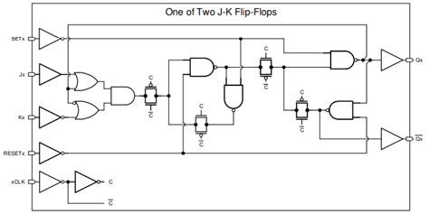
The CD4027 is a CMOS integrated circuit containing two independent J-K flip-flops. Each flip-flop has independent J, K, clock, set and reset inputs and Q and Q̅ outputs. The CD4027 is a versatile and widely used component in digital logic circuits for applications such as counters, shift registers, state machines, and data synchronization.
Key features of the CD4027 include:
– Dual J-K flip-flops in a single 16-pin package
– Wide supply voltage range of 3V to 15V
– High noise immunity
– Low power consumption
– Fully static operation – no minimum clock frequency
– Buffered outputs can drive up to 10 LSTTL loads
In this comprehensive guide, we’ll cover everything you need to know to effectively utilize the CD4027 in your designs, including pinout, function tables, timing diagrams, example circuits, and frequently asked questions. By the end of this article, you’ll have a solid understanding of how to integrate the CD4027 into your projects.
CD4027 Pinout and Pin Functions
The CD4027 comes in a 16-pin DIP or SOIC package. Here is the pinout:
| Pin | Name | Function |
|---|---|---|
| 1 | J1 | J input for flip-flop 1 |
| 2 | CLK1 | Clock input for flip-flop 1 |
| 3 | K1 | K input for flip-flop 1 |
| 4 | Q1 | Q output for flip-flop 1 |
| 5 | /Q1 | Inverted Q output for flip-flop 1 |
| 6 | Set1 | Set input for flip-flop 1 (active high) |
| 7 | Reset1 | Reset input for flip-flop 1 (active high) |
| 8 | VSS | Ground (0V) |
| 9 | Reset2 | Reset input for flip-flop 2 (active high) |
| 10 | Set2 | Set input for flip-flop 2 (active high) |
| 11 | /Q2 | Inverted Q output for flip-flop 2 |
| 12 | Q2 | Q output for flip-flop 2 |
| 13 | K2 | K input for flip-flop 2 |
| 14 | CLK2 | Clock input for flip-flop 2 |
| 15 | J2 | J input for flip-flop 2 |
| 16 | VDD | Positive supply voltage (3V to 15V) |
Each flip-flop has its own J, K, clock, set, and reset inputs that control the state and output. The Q and /Q outputs provide the current state of the flip-flop.

CD4027 Function Table
The state of a J-K flip-flop is determined by the J and K inputs at the rising edge of the clock signal. Here is the function table:
| J | K | Qn+1 | Action |
|---|---|---|---|
| 0 | 0 | Qn | Hold state |
| 0 | 1 | 0 | Reset |
| 1 | 0 | 1 | Set |
| 1 | 1 | /Qn | Toggle state |
Where:
– Qn is the current state of the flip-flop
– Qn+1 is the next state after the clock edge
– /Qn is the complement (inverse) of the current state
The set and reset inputs are asynchronous and override the J and K inputs. When set is high, the flip-flop is forced to the 1 state. When reset is high, it is forced to the 0 state. If both set and reset are high simultaneously, the output becomes unpredictable.

CD4027 Timing Diagram
Here is a timing diagram illustrating the operation of a single J-K flip-flop in the CD4027:
        ___________              ___________
CLK   _/           \_____________/           \___
       _____________________
J    __/                     \__________________
       _____________________
K    __/                     \__________________
            ___________________________
/Q    ______/                           \_______
        _____________________________
Q     _/                             \_________
At each rising edge of the clock (CLK), the J and K inputs determine the next state of the flip-flop outputs Q and /Q according to the function table. The outputs only change on the rising clock edge.
Set and reset assert asynchronously:
          ______________
Set     __/              \________________________
          ______________________
Reset  __/                      \________________
            ___________
/Q    ______/           \________________________
        ___________________
Q     _/                   \____________________
When set goes high, Q is forced high and /Q low regardless of the clock. Similarly, reset forces Q low and /Q high. The outputs remain in this state until the overriding input returns low.

Applications and Example Circuits
The CD4027 is used in a wide variety of digital circuits. Some common applications include:
Frequency Division
By connecting Q to K and /Q to J, a J-K flip-flop becomes a divide-by-two circuit. The output frequency is half the input clock frequency. Multiple divide-by-two stages can be cascaded for further division.
Modulo-n Counter
J-K flip-flops can be chained to create binary or BCD counters. The Q outputs represent the binary count. Combinational logic decodes states for modulo-n counters. Counters can be up, down, or up/down.
State Machines
J-K flip-flops store state bits in state machines. Combinational logic drives J-K inputs based on the current state and inputs to sequence to the next state.
Data Synchronization
Unsynchronized inputs to a sequential circuit can be synchronized to the clock by passing through a pair of cascaded flip-flops.
Shift Registers
J-K flip-flops pass data from J to Q on clock edges, useful for shifting data in serial-in, parallel-out or parallel-in, serial-out shift registers.
Here is an example 4-bit binary counter circuit using two CD4027s:
        Q0   Q1   Q2   Q3
      +--+--+--+--+--+--+
      |  |  |  |  |  |  |
+-----+  |  |  |  |  |  +-----+
|CLK0 >--+  |  |  |  |  |RESET+----> (ACTIVE HIGH)
+-----+     |  |  |  |  +-----+
             |  |  |  |
 +--------+  |  |  |  |
 |CD4027  |  |  |  |  |
 |J  CLK0 +--+  |  |  |
 |K  Q0---+-----+  |  |
 |Q       |        |  |
 |/Q      |        |  |
 |GND     |        |  |
 +--------+        |  |
             +--+  |  |
VCC  GND     |  |  |  |
+-+  +-+     |  |  |  +--------+
| |  | |     |  |  |  |CD4027  |
+-+  +-+     |  |  +--|J  CLK1 |
             |  +-----|K  Q1   |
             +------+-|Q       |
                      |/Q      |
                      |GND     |
                      +--------+
The Q outputs (Q0-Q3) form a 4-bit binary count sequence. The CLK0 input clocks the first flip-flop, and Q0 clocks the second flip-flop. The J and K inputs are tied to VCC and Q fed back to K, creating a toggle configuration for each stage. An active high reset input clears the counter when asserted.
By extending this design with more CD4027 packages, wider binary counts can easily be implemented. The Q outputs can drive additional logic for decoding or output.
CD4027 Electrical Characteristics
The CD4027 is designed for operation from 3V to 15V supplies. Here are some key electrical specifications:
| Parameter | Min | Typ | Max | Unit |
|---|---|---|---|---|
| Supply Voltage (VDD) | 3 | – | 15 | V |
| Input Voltage | 0 | – | VDD | V |
| Output Voltage | 0 | – | VDD | V |
| Input Current | – | – | 1 | μA |
| Output Current | – | – | ±1.6 | mA |
| Clock Frequency | 0 | – | 6 | MHz |
| Propagation Delay (tPHL) | – | 125 | 300 | ns |
| Propagation Delay (tPLH) | – | 150 | 300 | ns |
| Rise/Fall Time | – | 80 | 200 | ns |
| Quiescent Current (IDD) | – | 5 | 50 | μA |
As with all CMOS circuits, the power consumption is proportional to switching frequency. Faster clocks will consume more current. Unused inputs should be tied to VCC or GND to prevent floating and excess current draw.
CD4027 vs. Other J-K Flip-Flops
The CD4027 is one of several J-K flip-flop options. Here are some comparisons:
7473 (TTL)
- Dual J-K flip-flop like CD4027
- TTL compatible (5V only supply)
- Slightly faster than CD4027
- Higher power consumption
74HC73 (High Speed CMOS)
- Dual J-K flip-flop like CD4027
- CMOS with TTL compatible input thresholds
- 2V to 6V supply range
- Faster than 4027, slower than 7473
74HCT73 (High Speed TTL Compatible)
- Dual J-K flip-flop like CD4027
- CMOS core with TTL compatible inputs and outputs
- 4.5V to 5.5V supply range
- Faster than CD4027, speeds between 7473 and 74HC73
The CD4027 provides advantages in low power, wide supply range, and direct CMOS compatibility. The TTL 7473 and 74HCT73 are better choices when interfacing with TTL logic. The 74HC73 sits in the middle with improved speed over the 4027 while retaining a wider supply range. Choose the best fit for your particular application.
FAQs about the CD4027
Q: Can the CD4027 be used as a latch?
A: Yes. By holding the clock input high, the J-K inputs directly control the Q and /Q outputs, causing the flip-flop to act as a transparent latch.
Q: What happens if both set and reset are asserted?
A: If both set and reset inputs are high at once, the output state is unpredictable. This condition should be avoided. Only one overriding input should be active at a time.
Q: How do I calculate the output frequency of a CD4027 counter?
A: For ripple counters, the output frequency of each stage is half the frequency of the prior stage. For an n-stage counter, Fout = Fin / 2^n. Synchronous counters may use a different formula depending on the decoding logic.
Q: Why does my CD4027 draw excessive current?
A: Check that all inputs are at valid logic levels, not floating. Tie unused inputs high or low. Also verify the clock is within the rated frequency range. Excessively high clock speeds increase current consumption.
Q: Can I replace a 7473 with a CD4027?
A: It depends. CD4027 has slower speed ratings and may not be a drop-in replacement in high speed designs. Also ensure the logic levels are compatible or level shifted appropriately between the different IC families.
Conclusion
The CD4027 dual J-K flip-flop is a flexible building block for many digital designs. Its wide supply voltage range, low power consumption, and static architecture make it suitable for a variety of applications from simple data storage to complex state machines.
By understanding the function table, timing diagrams, and example circuits, you can effectively utilize the CD4027 in your projects. Consider the electrical specifications and compare with similar flip-flop ICs to select the optimal fit for your system.
We hope this comprehensive guide has equipped you with the knowledge to confidently incorporate the CD4027 in your digital logic designs. Always consult the official datasheet for your specific CD4027 variant for full details. Happy designing!


Leave a Reply