Introduction to PCB and 32 Layer PCBs
A Printed Circuit Board (PCB) is a fundamental component in modern electronics. It is a flat board made of insulating material, such as fiberglass or composite epoxy, with conductive pathways etched or printed onto its surface. These pathways, known as traces, connect various electronic components mounted on the board, allowing for complex circuits to be built in a compact and organized manner.
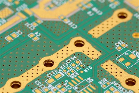
PCBs come in various types and configurations, differing in the number of layers, materials used, and manufacturing processes employed. One such type is the 32 layer PCB, which, as the name suggests, consists of 32 conductive layers sandwiched between insulating layers. This high layer count allows for extremely complex and dense circuit designs, making 32 layer PCBs a popular choice for advanced applications in industries such as aerospace, military, and high-performance computing.
Advantages of 32 Layer PCBs
-
High Density: The 32 layers allow for a large number of components and traces to be packed into a relatively small area, enabling the creation of highly complex circuits.
-
Improved Signal Integrity: With proper design techniques, the multiple layers can be used to reduce crosstalk and electromagnetic interference (EMI), leading to better signal integrity.
-
Increased Functionality: The high layer count enables the integration of multiple functions and subsystems onto a single board, reducing the need for separate PCBs and connectors.
-
Reduced Size and Weight: By consolidating multiple circuits onto a single board, 32 layer PCBs can help reduce the overall size and weight of electronic devices.
Challenges in 32 Layer PCB Design and Manufacturing
-
Complexity: Designing a 32 layer PCB requires advanced skills and tools due to the intricate layout and the need to manage signal integrity across multiple layers.
-
Manufacturing Difficulties: The high layer count and dense layouts can pose challenges during the manufacturing process, requiring specialized equipment and expertise.
-
Increased Cost: Due to the complexity of design and manufacturing, 32 layer PCBs are generally more expensive than boards with fewer layers.
-
Thermal Management: With a high density of components and traces, proper thermal management becomes crucial to ensure reliable operation and prevent overheating.
PCB Layer Stackup and Materials
Understanding PCB Layer Stackup
A PCB layer stackup refers to the arrangement of conductive and insulating layers within a PCB. In a 32 layer PCB, the stackup typically consists of alternating layers of copper (conductive) and prepreg (insulating) materials. The copper layers are used for signal routing, power distribution, and grounding, while the prepreg layers provide electrical isolation and mechanical support.
The stackup design plays a crucial role in determining the electrical performance and manufacturability of the PCB. Factors such as the thickness of the copper and prepreg layers, the spacing between layers, and the arrangement of signal, power, and ground planes all contribute to the overall performance of the board.
Common Materials Used in 32 Layer PCBs
-
FR-4: A composite material made of woven fiberglass cloth with an epoxy resin binder. FR-4 is the most widely used material for PCBs due to its good electrical and mechanical properties, as well as its affordability.
-
High-Tg FR-4: A variant of FR-4 with a higher glass transition temperature (Tg), which improves its thermal stability and resistance to warping during high-temperature assembly processes.
-
Rogers Materials: High-performance dielectric materials, such as Rogers RO4000 series, offer superior electrical properties, including low dielectric constant and low loss tangent, making them suitable for high-frequency applications.
-
Isola Materials: Isola offers a range of laminate and prepreg materials designed for high-speed digital and RF applications, with properties such as low dielectric constant, low loss tangent, and controlled impedance.
-
Copper: Copper foils of varying thicknesses are used for the conductive layers, with the most common thicknesses being 0.5 oz (17 µm), 1 oz (35 µm), and 2 oz (70 µm). Higher copper weights can be used for power and ground planes to improve current-carrying capacity.
Importance of Material Selection
Choosing the right materials for a 32 layer PCB is essential to ensure optimal performance, reliability, and manufacturability. Factors to consider when selecting materials include:
-
Electrical Properties: Dielectric constant, loss tangent, and dielectric strength should be chosen based on the application requirements, such as signal speed, frequency, and voltage.
-
Thermal Properties: Glass transition temperature (Tg) and coefficient of thermal expansion (CTE) should be considered to ensure the PCB can withstand the thermal stresses encountered during assembly and operation.
-
Mechanical Properties: The materials should provide sufficient mechanical strength and stability to support the components and withstand the stresses of handling and use.
-
Cost and Availability: The cost and availability of materials should be balanced against performance requirements to ensure the design is economically viable and can be manufactured consistently.

Design Considerations for 32 Layer PCBs
Signal Integrity
Signal integrity is a critical concern in 32 layer PCBs due to the high density of traces and the potential for crosstalk and EMI. To maintain signal integrity, designers should consider the following:
-
Controlled Impedance: Ensure that the characteristic impedance of the traces matches the impedance of the source and load to minimize reflections and signal distortion.
-
Trace Routing: Use appropriate trace widths and spacing to minimize crosstalk and maintain consistent impedance. Avoid sharp bends and long parallel runs of traces on adjacent layers.
-
Via Design: Optimize via placement and design to minimize signal degradation and reflections. Use appropriate via sizes and anti-pad diameters to control impedance and prevent signal coupling.
-
Layer Arrangement: Arrange signal layers to minimize crosstalk and EMI. Use ground and power planes to provide shielding and reduce noise coupling between layers.
Power Integrity
Maintaining power integrity is crucial to ensure stable and reliable operation of the components on the PCB. Key considerations include:
-
Power Distribution Network (PDN): Design a robust PDN with low impedance and sufficient current-carrying capacity to meet the power requirements of the components.
-
Decoupling Capacitors: Place decoupling capacitors close to power pins of components to minimize power supply noise and transient currents.
-
Plane Capacitance: Utilize the capacitance between power and ground planes to provide additional decoupling and reduce power supply noise.
-
Via Placement: Optimize the placement of power and ground vias to minimize voltage drops and ensure uniform power distribution across the board.
Thermal Management
With the high density of components and traces in a 32 layer PCB, proper thermal management is essential to prevent overheating and ensure reliable operation. Strategies for thermal management include:
-
Thermal Vias: Use thermal vias to conduct heat away from hot components and into the inner layers or the opposite side of the board.
-
Copper Pours: Use large copper pours on the outer layers to spread heat and improve heat dissipation.
-
Thermal Interface Materials (TIMs): Use TIMs, such as thermal pads or thermal adhesives, to enhance heat transfer between components and the PCB.
-
Airflow and Cooling: Consider the use of heatsinks, fans, or other cooling solutions to improve airflow and heat dissipation in the final assembly.
Design for Manufacturing (DFM)
To ensure the manufacturability and reliability of a 32 layer PCB, designers should follow DFM guidelines, such as:
-
Minimum Feature Sizes: Adhere to the minimum trace widths, spacings, and via sizes specified by the PCB manufacturer to ensure reliable fabrication.
-
Soldermask and Silkscreen: Provide adequate clearances for soldermask and silkscreen to prevent short circuits and improve the legibility of component markings.
-
Panelization: Consider the panel size and layout when designing the PCB to maximize manufacturing efficiency and minimize waste.
-
Testing and Inspection: Incorporate test points and fiducials to facilitate automated optical inspection (AOI) and in-circuit testing (ICT) during manufacturing.

Advanced Techniques for 32 Layer PCB Design
High-Speed Design
Designing for high-speed signals in a 32 layer PCB requires special considerations to maintain signal integrity and minimize EMI. Techniques for high-speed design include:
-
Differential Pairs: Use differential signaling for high-speed data transmission to reduce noise and improve signal quality.
-
Impedance Matching: Match the impedance of traces, vias, and connectors to minimize reflections and signal distortion.
-
Length Matching: Match the lengths of traces within a differential pair or a bus to ensure synchronous arrival of signals at the receiver.
-
Ground Referencing: Provide continuous ground reference planes adjacent to high-speed signal layers to minimize EMI and maintain consistent impedance.
RF and Microwave Design
32 layer PCBs can be used for RF and microwave applications, which require special design techniques to manage signal propagation and minimize losses. Some key considerations include:
-
Material Selection: Use low-loss dielectric materials, such as Rogers or Isola materials, to minimize signal attenuation and maintain consistent dielectric properties.
-
Controlled Impedance: Design traces and structures with controlled impedance to match the impedance of RF components and minimize reflections.
-
Grounding and Shielding: Use ground planes and shielding structures to minimize EMI and prevent unwanted coupling between RF signals.
-
Stripline and Microstrip: Use stripline and microstrip transmission line structures to guide RF signals and maintain consistent impedance.
Embedded Components
Embedding components within the layers of a 32 layer PCB can help reduce the surface area required for component placement and improve electrical performance. Techniques for embedded component design include:
-
Embedded Capacitors: Use the capacitance between power and ground planes to create embedded decoupling capacitors, reducing the need for surface-mounted components.
-
Embedded Resistors: Use resistive materials, such as thin-film or thick-film resistors, to create embedded resistors within the PCB layers.
-
Embedded Inductors: Use the inherent inductance of traces and vias to create embedded inductors for power management and filtering applications.
-
Cavity Embedding: Create cavities within the PCB layers to accommodate components, such as ICs or sensors, allowing for a more compact and integrated design.

Manufacturing and Assembly of 32 Layer PCBs
PCB Fabrication Process
The fabrication of a 32 layer PCB involves a complex process that requires specialized equipment and expertise. The main steps in the fabrication process include:
-
Inner Layer Printing: The copper foils for the inner layers are patterned using photolithography and etching processes.
-
Lamination: The patterned inner layers are stacked with prepreg layers and copper foils for the outer layers, then subjected to high temperature and pressure to bond them together.
-
Drilling: Holes are drilled through the laminated board for vias, component mounting, and tooling.
-
Plating: The drilled holes are plated with copper to create electrical connections between layers.
-
Outer Layer Patterning: The outer layer copper foils are patterned using photolithography and etching processes.
-
Soldermask and Silkscreen: Soldermask is applied to protect the copper traces, and silkscreen is used to add component markings and identifiers.
-
Surface Finish: A surface finish, such as HASL, ENIG, or OSP, is applied to protect the exposed copper and enhance solderability.
Assembly Processes
The assembly of components onto a 32 layer PCB involves several steps, including:
-
Solder Paste Printing: Solder paste is applied to the pads on the PCB using a stencil or screen printing process.
-
Component Placement: Components are placed onto the solder paste using automated pick-and-place machines or manual placement for larger components.
-
Reflow Soldering: The PCB with components is passed through a reflow oven, where the solder paste melts and forms electrical and mechanical bonds between the components and the PCB.
-
Inspection and Testing: The assembled PCB is inspected using automated optical inspection (AOI) and subjected to in-circuit testing (ICT) to verify proper assembly and functionality.
-
Rework and Repair: Any defects or issues identified during inspection and testing are corrected through rework and repair processes.
Quality Control and Reliability Testing
To ensure the quality and reliability of 32 layer PCBs, manufacturers employ various quality control and testing methods, such as:
-
Visual Inspection: Boards are visually inspected for defects, such as misaligned components, solder bridges, or damaged traces.
-
Automated Optical Inspection (AOI): Automated systems are used to quickly scan the PCB for assembly defects and anomalies.
-
X-Ray Inspection: X-ray imaging is used to inspect the internal layers and vias for defects, such as voids or cracks.
-
In-Circuit Testing (ICT): Electrical tests are performed to verify the continuity and functionality of the PCB and its components.
-
Environmental Testing: PCBs are subjected to environmental stresses, such as temperature cycling, humidity, and vibration, to assess their reliability under real-world conditions.
Applications of 32 Layer PCBs
High-Performance Computing
32 layer PCBs are commonly used in high-performance computing applications, such as:
-
Servers and Data Centers: The high density and signal integrity of 32 layer PCBs enable the design of compact and powerful server boards and data center equipment.
-
Supercomputers: The complex interconnects and high-speed interfaces required for supercomputers can be realized using 32 layer PCBs.
-
AI and Machine Learning: The processing power and bandwidth demanded by AI and machine learning applications can be met using 32 layer PCBs with high-speed processors and memory interfaces.
Aerospace and Defense
32 layer PCBs are used in various aerospace and defense applications due to their ability to support complex systems and withstand harsh environments. Examples include:
-
Avionics: The high density and reliability of 32 layer PCBs make them suitable for avionics systems, such as flight control, navigation, and communication equipment.
-
Radar and Electronic Warfare: The high-frequency performance and EMI shielding provided by 32 layer PCBs are essential for radar and electronic warfare systems.
-
Satellite Systems: The compact size and high functionality of 32 layer PCBs are valuable for satellite systems, where space and weight are at a premium.
Medical Devices
32 layer PCBs are used in advanced medical devices that require high-density interconnects and reliable performance, such as:
-
Diagnostic Imaging Equipment: The complex signal processing and data acquisition required for imaging equipment, such as MRI and CT scanners, can be implemented using 32 layer PCBs.
-
Implantable Devices: The compact size and high reliability of 32 layer PCBs make them suitable for implantable medical devices, such as pacemakers and neurostimulators.
-
Robotic Surgery Systems: The precise control and sensing required for robotic surgery systems can be achieved using 32 layer PCBs with high-speed interfaces and embedded components.
Frequently Asked Questions (FAQ)
-
Q: What is the typical turnaround time for a 32 layer PCB?
A: The turnaround time for a 32 layer PCB can vary depending on the complexity of the design, the manufacturing process, and the manufacturer’s workload. Typically, the fabrication and assembly of a 32 layer PCB can take several weeks, with lead times ranging from 3 to 8 weeks or more. -
Q: How much does a 32 layer PCB cost compared to a PCB with fewer layers?
A: The cost of a 32 layer PCB is significantly higher than that of a PCB with fewer layers due to the increased complexity of the design, the additional materials required, and the specialized manufacturing processes involved. The exact cost difference can vary depending on the specific design requirements and the manufacturer, but a 32 layer PCB can cost several times more than a comparable PCB with fewer layers. -
Q: Can 32 layer PCBs be reworked or repaired if defects are found?
A: While it is possible to rework or repair 32 layer PCBs, the process is more challenging and time-consuming compared to PCBs with fewer layers. The high density of interconnects and the presence of embedded components can make it difficult to access and repair specific areas of the board. Specialized equipment and expertise are often required for successful rework and repair of 32 layer PCBs. -
Q: Are there any limitations on the component types that can be used on a 32 layer PCB?
A: In general, most common component types can be used on a 32 layer PCB, including surface-mount devices (SMDs), through-hole components, and ball grid arrays (BGAs). However, the high density of interconnects and the limited space available on the surface of the board may restrict the size and pitch of the components that can be used. Designers should consult with the PCB manufacturer to ensure that the chosen components are compatible with the 32 layer PCB design and manufacturing process. -
**Q: What are the key challenges in achieving high yields


Leave a Reply