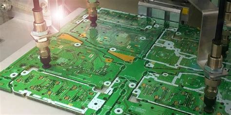
What is a PCB Annular Ring?
A PCB annular ring, also known as a pad or land, is the copper area that surrounds a drilled hole on a printed circuit board (PCB). The annular ring provides electrical connectivity between the component lead or pin inserted into the hole and the copper traces on the surface of the PCB. The size and shape of the annular ring play a critical role in the reliability and manufacturability of the PCB.
Why are PCB Annular Rings Important?
PCB annular rings serve several important functions:
-
Electrical Connection: The primary purpose of an annular ring is to provide a reliable electrical connection between the component lead and the copper trace on the PCB surface. A larger annular ring offers a greater contact area, ensuring a more robust connection.
-
Mechanical Strength: Annular rings also provide mechanical support to the component leads. A larger ring distributes the stress more evenly, reducing the risk of the lead breaking or the pad lifting off the PCB surface.
-
Manufacturing Tolerance: Annular rings help accommodate manufacturing tolerances. Drilling holes in PCBs is not an exact science, and there may be slight variations in hole size and position. A larger annular ring provides a greater margin for error, ensuring that the hole still makes proper contact with the copper pad.
Factors Affecting PCB Annular Ring Design
Several factors influence the design of PCB annular rings:
Hole Size
The size of the drilled hole determines the minimum size of the annular ring. The hole must be large enough to accommodate the component lead while leaving sufficient copper around the hole for electrical and mechanical integrity.
PCB Thickness
The thickness of the PCB also affects annular ring design. Thicker boards require larger holes to maintain the proper aspect ratio, which in turn requires larger annular rings.
Copper Weight
The weight of the copper on the PCB surface impacts the annular ring size. Heavier copper weights allow for smaller annular rings, as the thicker copper provides better electrical and mechanical properties.
Manufacturing Capabilities
The capabilities of the PCB manufacturer also play a role in annular ring design. Some manufacturers may have tighter tolerances and more advanced equipment, allowing for smaller annular rings.

PCB Annular Ring Size Guidelines
The following table provides general guidelines for annular ring sizes based on hole size:
| Hole Size (mm) | Minimum Annular Ring (mm) |
|---|---|
| 0.2 – 0.5 | 0.15 |
| 0.5 – 1.0 | 0.20 |
| 1.0 – 2.0 | 0.25 |
| 2.0 – 4.0 | 0.30 |
| 4.0 – 6.0 | 0.40 |
It’s important to note that these are minimum values, and larger annular rings may be necessary depending on the specific application and manufacturing requirements.
Common PCB Annular Ring Issues
Several issues can arise with PCB annular rings:
Insufficient Annular Ring
If the annular ring is too small, it may not provide adequate electrical or mechanical connection. This can lead to intermittent connections, signal integrity issues, or component failure.
Pad Lifting
Pad lifting occurs when the annular ring separates from the PCB surface. This can be caused by thermal stress, mechanical stress, or poor adhesion between the copper and the PCB substrate. Proper annular ring design and manufacturing processes can help prevent pad lifting.
Solder Bridging
Solder bridging occurs when solder inadvertently connects adjacent pads. This can be caused by excessive solder, improper solder mask design, or insufficient spacing between pads. Proper annular ring design and solder mask application can help mitigate solder bridging.
Best Practices for PCB Annular Ring Design
To ensure optimal PCB annular ring design, consider the following best practices:
-
Consult with your PCB manufacturer early in the design process to understand their capabilities and limitations.
-
Use the largest annular rings possible, within the constraints of your design and manufacturing capabilities.
-
Ensure proper spacing between annular rings to prevent solder bridging and signal integrity issues.
-
Use appropriate solder mask coverage to prevent solder bridging and protect the annular rings.
-
Consider the thermal and mechanical stresses your PCB will be subjected to, and design your annular rings accordingly.
FAQ
Q1: What is the difference between an annular ring and a pad?
A1: Annular ring and pad are often used interchangeably, but technically, the annular ring refers specifically to the copper area surrounding a drilled hole, while a pad can refer to any copper area on the PCB surface, whether or not it has a hole.
Q2: Can I use different annular ring sizes on the same PCB?
A2: Yes, you can use different annular ring sizes for different components or holes on the same PCB. This is often necessary to accommodate different component sizes and lead diameters.
Q3: What happens if my annular ring is too small?
A3: If the annular ring is too small, it may not provide adequate electrical or mechanical connection. This can lead to intermittent connections, signal integrity issues, or component failure.
Q4: How do I prevent pad lifting?
A4: Proper annular ring design and manufacturing processes can help prevent pad lifting. This includes using appropriate copper weights, ensuring good adhesion between the copper and the PCB substrate, and minimizing thermal and mechanical stresses.
Q5: Can I use non-circular annular rings?
A5: While circular annular rings are the most common, some designs may require non-circular shapes, such as rectangles or ovals. However, non-circular annular rings can be more challenging to manufacture and may require special considerations for drilling and plating.
Conclusion
PCB annular rings play a critical role in the reliability and manufacturability of printed circuit boards. Proper annular ring design ensures robust electrical and mechanical connections, accommodates manufacturing tolerances, and helps prevent issues such as pad lifting and solder bridging. By understanding the factors that affect annular ring design and following best practices, designers can create PCBs that are reliable, manufacturable, and meet the specific needs of their applications.


Leave a Reply