Introduction to Voltage Doubler Circuits
A voltage doubler is an electronic circuit that converts AC electrical power from a lower voltage to a higher DC voltage, typically doubling the input voltage. It achieves this using a combination of diodes and capacitors. Voltage doubler circuits offer a cheaper, lighter, and more compact alternative to bulky transformer-Rectifier Circuits for low-power applications requiring higher DC voltages than are available from the AC mains supply.
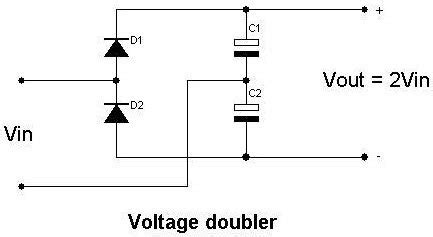
How a Basic Voltage Doubler Works
A basic voltage doubler circuit consists of two diodes and two capacitors arranged so that the capacitors are charged on alternating half-cycles of the AC input voltage. The key components are:
- Two diodes (D1 & D2) – Rectify the AC input, only allowing current to flow in one direction
- Two capacitors (C1 & C2) – Store charge and smooth the output DC voltage
Here is a schematic diagram of a basic voltage doubler circuit:
        +----|>|-----+-----|>|------+
  AC    |    D1      |     D2       |
 Input  =            =              |
        |    C1      |     C2       |    DC
        =            =              |   Output
        |            |              |
  --    +------------+--------------+
On the first half-cycle of the AC input, D1 conducts and C1 is charged up to the peak voltage (Vpk) of the input. On the next half-cycle, the input voltage reverses polarity. The series combination of the input and the voltage across C1 (which is now 2Vpk) is applied to C2 and D2, charging C2 to 2Vpk. The voltage across C2 is the circuit output voltage.
This doubling action is summarized in the table below:
| Half-Cycle | D1 | D2 | C1 Voltage | C2 Voltage |
|---|---|---|---|---|
| 1st | On | Off | Vpk | – |
| 2nd | Off | On | – | 2Vpk |
The main advantages of this circuit are:
- Simple design using few components
- Lightweight and compact
- Cheaply doubles the input voltage
- Works for a wide frequency range
Voltage Doubler Applications
Voltage doublers are commonly used in electronic circuits where a higher DC voltage is required than is available from the power supply. Typical applications include:
- Generating +/-15V rails from a 9V AC adapter in analog audio gear
- Providing high voltage for Geiger counters, photoflash capacitors, and strobe lights
- Biasing photomultiplier tubes and avalanche photodiodes
- DC-DC converters in battery-powered equipment
- Driving nixie tubes for retro displays
Voltage Doubler Circuit Design Considerations
When designing a practical voltage doubler circuit for a given application, there are several factors to consider:
Required Output Voltage and Current
The output voltage of an unloaded ideal voltage doubler is twice the peak input voltage. However, in practice the output voltage will be somewhat less, depending on:
- Diode forward voltage drops
- Capacitor value and ESR losses
- Load current drawn from the output
A rule of thumb is the output voltage will be roughly 1.8 to 1.9 times the RMS input voltage under light loading. The ripple voltage will increase with increasing load current for a given capacitor value.
Diode Selection
The diodes used in voltage doubler circuits must be rated to handle the peak input voltage plus transient spikes, and the maximum load current. Schottky diodes are often used for their low forward voltage drop. For high frequency designs, fast recovery diodes may be required.
Capacitor Selection
The capacitor values required depend on the acceptable ripple voltage at the required load current. Larger capacitances will give lower output ripple. The capacitors must be rated for at least twice the peak input voltage, preferably with some safety margin. Low ESR types are preferable to minimize resistive losses and heat generation.
Input and Output Filtering
Depending on the application, some filtering of the input and output waveforms may be required:
- An LC low-pass filter before the doubler will attenuate high frequency harmonics and limit EMI.
- A pi-filter after the doubler will further reduce output ripple and noise.
Care must be taken not to resonant the input filter with the doubler capacitances at the power frequency.

Voltage Doubler Variants
Several variations of the basic voltage doubler circuit exist to output higher voltages or provide regulation:
Cascade Voltage Multipliers
Connecting multiple voltage doubler stages in series yields even higher output voltages in multiples of 2Vpk. These circuits are referred to as cascade multipliers. For example:
- Two stages gives a quadrupler (4Vpk output)
- Three stages gives an octupler (8Vpk output)
And so on in powers of two. An n-stage cascade multiplier will ideally output 2^n times the peak input voltage. The disadvantages of cascading many stages include:
- Increased component count and size
- Higher output impedance and poorer regulation
- Slower transient response
Cascaded doublers are used where very high voltages are needed, such as in particle accelerators and X-ray machines.
Symmetrical Voltage Doublers
For applications requiring a bipolar output voltage, a symmetrical circuit using four diodes can be used. It generates equal positive and negative output voltages with respect to ground. Here is the schematic:
       +--|>|---+---|>|--+
  AC   |  D1    |   D2   |
 Input
       +-|<|--+-----|<|-+
          D3  |  +  D4  |
              |  C1     |
              =         =
              |         |
              +---------+
                  ||
                 -  +
The output is taken across C1, which is charged to +/-Vpk on alternate half-cycles via the diode bridge. Useful for analog audio and other applications requiring bipolar supply rails.
Regulated Voltage Doublers
The output of a basic doubler varies with input voltage and load current. For applications requiring a more stable supply, some form of regulation can be added:
- A simple linear regulator or Zener clamp to set the output voltage
- A switch-mode DC-DC converter for improved efficiency
- An active doubler design using op-amps for lower output impedance
Regulation is at the expense of increased circuit complexity and cost.

Voltage Doubler Design Examples
Here are some practical voltage doubler design examples highlighting component choices and expected performance:
9V AC to +/-15V 30mA Bipolar Supply
- Input: 9V RMS 60Hz AC
- Output: +/-15V 30mA
- Diodes: 1N5819 40V 1A Schottky
- Capacitors: 470uF 35V electrolytic
- Linear Regulators: 7815 +15V, 7915 -15V
120V AC to 170V DC 50mA Photoflash Supply
- Input: 120V RMS 60Hz AC
- Output: 170V 50mA
- Diodes: 1N4007 1000V 1A
- Capacitors: 100uF 250V electrolytic
- Bleeder resistor: 100k 2W
5V USB to 10V 100mA Nixie Supply
- Input: 5V 500mA USB power
- Output: 10V 100mA
- Diodes: BAT54 30V 200mA Schottky
- Capacitors: 22uF 16V ceramic
- DC-DC Converter: MC34063 or equivalent
These are just a few examples of the wide range of voltage doubler solutions. When choosing components, allow sufficient voltage and current margins, and verify power dissipation and temperature rise.

Voltage Doubler FAQ
Q: How much current can a voltage doubler supply?
A: This depends on the diodes and capacitors used and the acceptable output voltage drop. Higher current requires larger capacitance values, lower ESR, and diodes rated for the maximum load. With appropriate components, currents of hundreds of mA or more are possible.
Q: What is the efficiency of a voltage doubler?
A: The conversion efficiency is limited by the diode forward voltage drops, capacitor ESR losses, and the ratio of output to input voltage. Basic doublers range from about 70-95% efficiency depending on the components used and operating conditions. Synchronous rectification and active designs can improve efficiency.
Q: Can a voltage doubler operate from a DC input?
A: No, doublers rely on the alternating polarity of an AC input to function. However, a DC-AC inverter can be used to generate AC from a DC source, which can then be doubled. Alternatively, a dedicated switched capacitor DC-DC converter IC can directly generate higher voltage outputs from a DC input.
Q: How does the output voltage change with loading?
A: The output voltage of a doubler will drop as load current increases due to the combined effect of capacitor discharge between AC peaks and diode and ESR voltage drops. The regulation (i.e. the change in output voltage from zero to full load) depends on the capacitance value and ESR. Regulation can be improved by larger capacitances, lower ESR, or by adding a linear or switching post-regulator.
Q: What are the input frequency limits of a voltage doubler?
A: Theoretically, doublers can operate from near DC up to several MHz, but most practical designs are limited to 50/60Hz line frequency up to a few hundred kHz due to the available ranges of suitable diodes and capacitors. The capacitor values required for a given ripple voltage are inversely proportional to frequency. At high frequencies, fast diodes with low stored charge are required. Parasitic inductances also become increasingly critical to minimize at higher frequencies.
Conclusion
Voltage doubler circuits offer a simple, low-cost solution for generating higher DC voltages from lower AC inputs without the bulk and expense of a transformer. While they have some limitations in output current and regulation, a well-designed doubler using appropriate components can be suitable for many cost-sensitive or low-power applications requiring a high voltage rail. Understanding the operating principle, design trade-offs, and component selection criteria enables choosing the best doubler configuration to meet a given set of requirements.


Leave a Reply