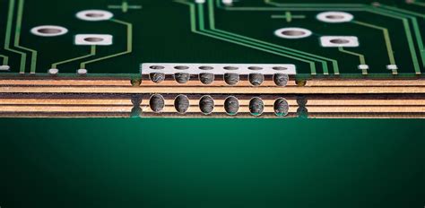
What is PCB Cross-Section Analysis?
PCB cross-section analysis is a process that involves cutting a small portion of a printed circuit board and examining its internal structure using microscopic imaging techniques. This allows engineers to observe the various layers, components, and interconnections within the PCB, providing valuable insights into its manufacturing quality and potential failure points.
The primary goals of PCB cross-section analysis include:
- Verifying the integrity of the PCB’s internal structure
- Identifying manufacturing defects or inconsistencies
- Evaluating the quality of the materials used
- Investigating the causes of PCB failures
- Validating the PCB design and ensuring compliance with industry standards
Techniques Used in PCB Cross-Section Analysis
Sample Preparation
To perform PCB cross-section analysis, a small sample of the PCB must be carefully prepared. This process typically involves the following steps:
-
Cutting: A small portion of the PCB is cut using a precision saw or Laser Cutter. The cut is made perpendicular to the surface of the board to expose its internal layers.
-
Mounting: The PCB sample is then mounted in a special resin or epoxy material to stabilize it during the subsequent grinding and polishing processes.
-
Grinding and Polishing: The mounted sample is gradually ground and polished using progressively finer abrasive materials until a smooth, mirror-like surface is achieved. This process reveals the internal structure of the PCB in great detail.
-
Etching: In some cases, the polished sample may be etched with a chemical solution to enhance the contrast between different materials and layers, making them more easily distinguishable under the microscope.
Imaging Techniques
Once the PCB sample is prepared, various imaging techniques are used to examine its internal structure. These techniques include:
-
Optical Microscopy: Optical microscopes use visible light to magnify the PCB cross-section, allowing engineers to observe the layers, traces, and components in detail. This technique is suitable for low to medium magnifications (up to 1000x).
-
Scanning Electron Microscopy (SEM): SEM uses a focused beam of electrons to scan the surface of the PCB cross-section, producing high-resolution images with magnifications up to 100,000x. This technique is particularly useful for examining fine details and detecting minuscule defects.
-
Energy-Dispersive X-ray Spectroscopy (EDS): EDS is often used in conjunction with SEM to analyze the chemical composition of materials within the PCB. This technique can help identify contaminants, material inconsistencies, or improper plating.
-
Focused Ion Beam (FIB): FIB uses a focused beam of ions to mill away specific areas of the PCB cross-section, allowing for targeted analysis of specific components or features. This technique is particularly useful for investigating localized defects or failures.

Applications of PCB Cross-Section Analysis
PCB cross-section analysis has numerous applications throughout the lifecycle of a printed circuit board, from design and manufacturing to failure analysis and quality control.
Design Validation
During the design phase, PCB cross-section analysis can be used to validate the proposed layer stack-up, trace widths, and spacing between components. By examining a prototype PCB’s cross-section, engineers can ensure that the design meets the required specifications and industry standards before mass production begins.
Manufacturing Quality Control
PCB cross-section analysis plays a crucial role in quality control during the manufacturing process. By regularly sampling and analyzing PCBs from production runs, manufacturers can identify and address any issues related to material quality, plating consistency, or process control. This helps to maintain high manufacturing standards and reduce the risk of defective products reaching customers.
Failure Analysis
When a PCB fails in the field, cross-section analysis is often used to investigate the cause of the failure. By examining the internal structure of the failed PCB, engineers can identify potential issues such as:
- Manufacturing defects (e.g., voids, delamination, or improper plating)
- Material degradation (e.g., thermal damage or chemical contamination)
- Design flaws (e.g., insufficient spacing between traces or components)
- Environmental factors (e.g., moisture ingress or mechanical stress)
By understanding the root cause of a failure, engineers can develop targeted solutions to prevent similar issues from occurring in the future.
Counterfeit Detection
PCB cross-section analysis can also be used to detect counterfeit components or materials. By comparing the internal structure of a suspect PCB with that of a genuine one, experts can identify discrepancies in material composition, layer thickness, or component placement, which may indicate a counterfeit product.

Industry Standards and Best Practices
Several industry standards and best practices govern the use of PCB cross-section analysis, ensuring consistent and reliable results across different organizations and applications. Some of the key standards include:
- IPC-A-600: Acceptability of Printed Boards
- IPC-6012: Qualification and Performance Specification for Rigid Printed Boards
- IPC-TM-650: Test Methods Manual
These standards provide guidelines for sample preparation, imaging techniques, and the interpretation of results, helping to maintain a high level of quality and consistency in PCB cross-section analysis.

Future Trends in PCB Cross-Section Analysis
As PCB technology continues to advance, cross-section analysis techniques must also evolve to keep pace with new challenges and requirements. Some of the future trends in PCB cross-section analysis include:
-
Automated Sample Preparation: The development of automated sample preparation systems can help to reduce the time and labor required for PCB cross-section analysis, while also improving the consistency and reliability of results.
-
High-Resolution Imaging: Advances in imaging technology, such as ultra-high resolution SEM and 3D X-ray tomography, will enable engineers to examine PCB cross-sections in even greater detail, potentially revealing previously undetectable defects or inconsistencies.
-
Machine Learning and AI: The application of machine learning and artificial intelligence algorithms to PCB cross-section analysis can help to automate the detection and classification of defects, reducing the need for manual interpretation and improving the speed and accuracy of results.
-
Integration with Other Analysis Techniques: Combining PCB cross-section analysis with other techniques, such as thermal imaging, acoustic microscopy, or electrical testing, can provide a more comprehensive understanding of a PCB’s performance and reliability.
Conclusion
PCB cross-section analysis is a vital tool for ensuring the quality, reliability, and performance of printed circuit boards. By examining the internal structure of a PCB, engineers and technicians can identify potential issues, validate designs, and investigate failures, ultimately leading to improved product quality and customer satisfaction.
As PCB technology continues to evolve, cross-section analysis techniques must also adapt to meet new challenges and requirements. By staying up-to-date with the latest industry standards, best practices, and emerging technologies, PCB professionals can leverage cross-section analysis to drive innovation and maintain a competitive edge in the ever-changing world of electronics manufacturing.
Frequently Asked Questions (FAQ)
-
What is the purpose of PCB cross-section analysis?
PCB cross-section analysis is used to examine the internal structure of a printed circuit board, allowing engineers to verify the integrity of the PCB’s layers, identify manufacturing defects, evaluate material quality, investigate failures, and validate the PCB design. -
What are the main steps involved in preparing a PCB sample for cross-section analysis?
The main steps in preparing a PCB sample for cross-section analysis include cutting a small portion of the board, mounting the sample in a special resin or epoxy, grinding and polishing the sample to reveal its internal structure, and, in some cases, etching the polished surface to enhance the contrast between different materials and layers. -
What imaging techniques are commonly used in PCB cross-section analysis?
The most common imaging techniques used in PCB cross-section analysis are optical microscopy, scanning electron microscopy (SEM), energy-dispersive X-ray spectroscopy (EDS), and focused ion beam (FIB) analysis. -
How can PCB cross-section analysis help detect counterfeit components or materials?
By comparing the internal structure of a suspect PCB with that of a genuine one, experts can identify discrepancies in material composition, layer thickness, or component placement, which may indicate a counterfeit product. -
What are some of the future trends in PCB cross-section analysis?
Future trends in PCB cross-section analysis include the development of automated sample preparation systems, advances in high-resolution imaging technologies, the application of machine learning and AI for defect detection and classification, and the integration of cross-section analysis with other analysis techniques for a more comprehensive understanding of PCB performance and reliability.
| Technique | Description | Maximum Magnification | Applications |
|---|---|---|---|
| Optical Microscopy | Uses visible light to magnify the PCB cross-section, allowing observation of layers, traces, and components. | 1000x | Low to medium magnification analysis, suitable for general inspection and documentation. |
| Scanning Electron Microscopy (SEM) | Uses a focused beam of electrons to scan the surface of the PCB cross-section, producing high-resolution images. | 100,000x | High magnification analysis, detection of minuscule defects, and fine details. |
| Energy-Dispersive X-ray Spectroscopy (EDS) | Used in conjunction with SEM to analyze the chemical composition of materials within the PCB. | N/A | Identification of contaminants, material inconsistencies, or improper plating. |
| Focused Ion Beam (FIB) | Uses a focused beam of ions to mill away specific areas of the PCB cross-section, allowing for targeted analysis of specific components or features. | N/A | Investigation of localized defects or failures. |


Leave a Reply