Introduction to ATMEGA8
The ATMEGA8 is a low-power, high-performance 8-bit microcontroller based on the AVR enhanced RISC architecture. It offers the following key features:
- 8KB of in-system programmable flash memory
- 1KB SRAM
- 512 bytes EEPROM
- 23 general-purpose I/O lines
- 32 general-purpose working registers
- Three flexible timer/counters with compare modes
- Internal and external interrupts
- Serial programmable USART
- SPI serial port
- 6-channel 10-bit ADC
- Programmable watchdog timer with internal oscillator
- Five software-selectable power-saving modes
With its rich set of features and capabilities, the ATMEGA8 is suitable for a wide range of applications, including automation, robotics, data logging, and more.
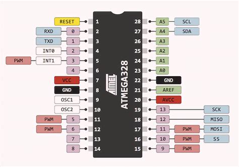
ATMEGA8 Pinout Overview
The ATMEGA8 comes in a 28-pin DIP (Dual Inline Package) or 32-pad QFN/MLF (Quad Flat No-Lead) package. Let’s take a closer look at the pinout of the DIP package:
| Pin | Name | Description |
|---|---|---|
| 1 | PC6 (RESET) | Reset input. A low level on this pin for longer than the minimum pulse length will generate a reset, even if the clock is not running. |
| 2 | PD0 (RXD) | USART input pin. |
| 3 | PD1 (TXD) | USART output pin. |
| 4 | PD2 (INT0) | External interrupt 0 input. |
| 5 | PD3 (INT1) | External interrupt 1 input. |
| 6 | PD4 (XCK/T0) | Timer/Counter0 external counter input. |
| 7 | VCC | Supply voltage. |
| 8 | GND | Ground. |
| 9 | PB6 (XTAL1/TOSC1) | Chip clock oscillator pin 1 or Timer/Counter0 oscillator pin 1. |
| 10 | PB7 (XTAL2/TOSC2) | Chip clock oscillator pin 2 or Timer/Counter0 oscillator pin 2. |
| 11 | PD5 (T1) | Timer/Counter1 external counter input. |
| 12 | PD6 (AIN0) | Analog comparator positive input. |
| 13 | PD7 (AIN1) | Analog comparator negative input. |
| 14 | PB0 (ICP) | Timer/Counter1 input capture pin. |
| 15 | PB1 (OC1A) | Timer/Counter1 output compare match A output. |
| 16 | PB2 (SS/OC1B) | SPI slave select input or Timer/Counter1 output compare match B output. |
| 17 | PB3 (MOSI/OC2) | SPI master output/slave input or Timer/Counter2 output compare match output. |
| 18 | PB4 (MISO) | SPI master input/slave output. |
| 19 | PB5 (SCK) | SPI bus master clock input. |
| 20 | AVCC | Supply voltage for ADC. |
| 21 | AREF | ADC reference voltage. |
| 22 | GND | Ground. |
| 23 | PC0 (ADC0) | ADC input channel 0. |
| 24 | PC1 (ADC1) | ADC input channel 1. |
| 25 | PC2 (ADC2) | ADC input channel 2. |
| 26 | PC3 (ADC3) | ADC input channel 3. |
| 27 | PC4 (ADC4/SDA) | ADC input channel 4 or I2C data line. |
| 28 | PC5 (ADC5/SCL) | ADC input channel 5 or I2C clock line. |
Power Supply
The ATMEGA8 requires a stable power supply to function correctly. The VCC pin (7) should be connected to a regulated power supply ranging from 2.7V to 5.5V. It’s essential to ensure that the power supply is clean and free from noise to avoid any issues with the microcontroller’s operation.
The AVCC pin (20) is the supply voltage for the ADC and should be connected to VCC through a low-pass filter. This helps to reduce noise and improve the accuracy of the ADC measurements.
Clock Sources
The ATMEGA8 supports various clock sources, including:
- External crystal/ceramic resonator
- External clock
- Internal calibrated RC oscillator
The most common clock source is an external crystal or ceramic resonator connected between the XTAL1 (PB6) and XTAL2 (PB7) pins. The frequency of the crystal/resonator can range from 1 MHz to 16 MHz.
If an external clock source is used, it should be connected to the XTAL1 (PB6) pin, while the XTAL2 (PB7) pin should be left unconnected.
The internal calibrated RC oscillator provides a clock frequency of 1 MHz, 2 MHz, 4 MHz, or 8 MHz, depending on the fuse settings. This clock source is useful when a precise clock frequency is not required, and it helps to reduce the external component count.
Reset
The RESET pin (PC6) is used to reset the microcontroller. A low level on this pin for longer than the minimum pulse length will generate a reset, even if the clock is not running. It’s recommended to connect a pull-up resistor (10k) between the RESET pin and VCC to ensure a stable reset condition.
I/O Ports
The ATMEGA8 has three I/O ports: PORTB, PORTC, and PORTD. Each port has 8 pins that can be configured as inputs or outputs. The direction of the pins is controlled by the corresponding Data Direction Register (DDR), while the state of the pins is read from or written to the Port Register (PORT).
Here’s a brief overview of each port:
PORTB
PORTB has 8 pins (PB0 to PB7) and is used for various purposes, such as:
- Timer/Counter1 input capture (PB0)
- Timer/Counter1 output compare match A (PB1)
- SPI slave select or Timer/Counter1 output compare match B (PB2)
- SPI master output/slave input or Timer/Counter2 output compare match (PB3)
- SPI master input/slave output (PB4)
- SPI bus master clock input (PB5)
- Chip clock oscillator or Timer/Counter0 oscillator (PB6 and PB7)
PORTC
PORTC has 6 pins (PC0 to PC5) and is primarily used for analog-to-digital conversion (ADC) and I2C communication. The specific functions of each pin are:
- ADC input channels 0 to 5 (PC0 to PC5)
- I2C data line (PC4)
- I2C clock line (PC5)
PORTD
PORTD has 8 pins (PD0 to PD7) and is used for various purposes, such as:
- USART input (PD0)
- USART output (PD1)
- External interrupts 0 and 1 (PD2 and PD3)
- Timer/Counter0 external counter input (PD4)
- Timer/Counter1 external counter input (PD5)
- Analog comparator positive and negative inputs (PD6 and PD7)
Serial Communication
The ATMEGA8 supports various serial communication protocols, including USART, SPI, and I2C.
USART
The Universal Synchronous and Asynchronous Receiver and Transmitter (USART) is a flexible serial communication interface that supports both synchronous and asynchronous modes. The USART pins are:
- RXD (PD0): USART input pin
- TXD (PD1): USART output pin
- XCK (PD4): USART external clock input/output
To use the USART, you need to configure the baud rate, data format, and other parameters using the UCSRA, UCSRB, UCSRC, UBRRL, and UBRRH registers.
SPI
The Serial Peripheral Interface (SPI) is a synchronous serial communication interface that provides high-speed data transfer between the ATMEGA8 and other SPI devices. The SPI pins are:
- SS (PB2): Slave select input
- MOSI (PB3): Master output/slave input
- MISO (PB4): Master input/slave output
- SCK (PB5): SPI bus master clock input
To use the SPI, you need to configure the SPI mode, clock rate, and other parameters using the SPCR and SPSR registers.
I2C
The Inter-Integrated Circuit (I2C) is a synchronous serial communication interface that allows the ATMEGA8 to communicate with other I2C devices using a two-wire bidirectional bus. The I2C pins are:
- SDA (PC4): I2C data line
- SCL (PC5): I2C clock line
To use the I2C, you need to configure the slave address, clock frequency, and other parameters using the TWBR, TWSR, TWAR, and TWCR registers.
Analog-to-Digital Converter (ADC)
The ATMEGA8 features a 6-channel, 10-bit analog-to-digital converter (ADC) that allows the microcontroller to measure analog signals and convert them into digital values. The ADC pins are:
- ADC0 to ADC5 (PC0 to PC5): ADC input channels
To use the ADC, you need to configure the reference voltage, input channel, prescaler, and other parameters using the ADMUX and ADCSRA registers. The ADC conversion result is stored in the ADCL and ADCH registers.

Getting Started with ATMEGA8
To start using the ATMEGA8 microcontroller, follow these steps:
- Connect the power supply (VCC and GND) to the appropriate pins.
- Connect the clock source (crystal, resonator, or external clock) to the XTAL1 and XTAL2 pins, if required.
- Configure the I/O pins as inputs or outputs using the DDR registers.
- Initialize the desired peripherals (USART, SPI, I2C, ADC, etc.) by setting the appropriate registers.
- Write your application code to interact with the peripherals and perform the desired tasks.
- Compile and upload the code to the ATMEGA8 using a programmer (e.g., AVRISP, USBASP, or Arduino ISP).
There are numerous development environments and tools available for programming the ATMEGA8, such as:
- Atmel Studio: A free, integrated development environment (IDE) provided by Atmel for developing and debugging AVR and SAM microcontroller applications.
- Arduino IDE: An open-source IDE that simplifies the process of writing and uploading code to AVR microcontrollers, including the ATMEGA8.
- avr-gcc: A free, open-source toolchain for compiling C/C++ code for AVR microcontrollers.

Example Projects
To help you get started with the ATMEGA8, here are a few example projects that demonstrate the use of various peripherals and features:
LED Blink
This simple project blinks an LED connected to one of the I/O pins.
#include <avr/io.h>
#include <util/delay.h>

#define LED_PIN PB0

int main(void)
{
    DDRB |= (1 << LED_PIN); // Set LED_PIN as output

    while (1)
    {
        PORTB |= (1 << LED_PIN); // Turn LED on
        _delay_ms(1000); // Wait for 1 second

        PORTB &= ~(1 << LED_PIN); // Turn LED off
        _delay_ms(1000); // Wait for 1 second
    }

    return 0;
}
Serial Communication
This project demonstrates how to send and receive data using the USART peripheral.
#include <avr/io.h>
#include <util/delay.h>
#include <stdio.h>

#define BAUD 9600
#define F_CPU 8000000UL
#define BAUD_PRESCALER (((F_CPU / (BAUD * 16UL))) - 1)

void USART_init(void);
void USART_send(char data);
char USART_receive(void);

int main(void)
{
    char data;
    USART_init();

    while (1)
    {
        data = USART_receive();
        USART_send(data);
    }

    return 0;
}

void USART_init(void)
{
    UBRRH = (uint8_t)(BAUD_PRESCALER >> 8);
    UBRRL = (uint8_t)(BAUD_PRESCALER);
    UCSRB = (1 << RXEN) | (1 << TXEN);
    UCSRC = (1 << URSEL) | (1 << UCSZ1) | (1 << UCSZ0);
}

void USART_send(char data)
{
    while (!(UCSRA & (1 << UDRE)));
    UDR = data;
}

char USART_receive(void)
{
    while (!(UCSRA & (1 << RXC)));
    return UDR;
}
ADC Measurement
This project demonstrates how to read an analog value using the ADC peripheral and send the result via USART.
“`c
include
include
include
define BAUD 9600
define F_CPU 8000000UL
define BAUD_PRESCALER (((F_CPU / (BAUD * 16UL))) – 1)
void USART_init(void);
void USART_send_string(char *str);
uint16_t ADC_read(uint8_t channel);
int main(void)
{
char buffer[10];
uint16_t adc_value;
USART_init();
ADMUX = (1 << REFS0); // Set ADC reference to AVCC
ADCSRA = (1 << ADEN) | (1 << ADPS2) | (1 << ADPS1) | (1 << ADPS0); // Enable ADC, set prescaler to 128

while (1)
{
    adc_value = ADC_read(0); // Read ADC value from channel 0
    sprintf(buffer, "%d\r\n", adc_value); // Convert the value to a string
    USART_send_string(buffer); // Send the string via USART
    _delay_ms(1000); // Wait for 1 second
}

return 0;
}
void USART_init(void)
{
UBRRH = (uint8_t)(BAUD_PRESCALER >> 8);
UBRRL = (uint8_t)(BAUD_PRESCALER);
UCSRB = (1 << RXEN) | (1 << TXEN);
UCSRC = (1 << URSEL) | (1 << UCSZ1) | (1 << UCSZ0);
}
void USART_send_string(char str)
{
while (str)
{
while (!(UCSRA & (1 << UDRE


Leave a Reply