Introduction to QFN Packaging
Quad Flat No-lead (QFN) packaging is a surface-mount technology that has gained significant popularity in the electronics industry due to its compact size, excellent thermal and electrical performance, and cost-effectiveness. QFN packages are widely used in various applications, including consumer electronics, automotive systems, and industrial devices.
In this article, we will explore the different types of QFN packages, their assembly process, and the benefits they offer compared to other packaging technologies.
Types of QFN Packages
Standard QFN Packages
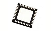
Standard QFN packages are the most common type and are characterized by their square or rectangular shape, with leads on all four sides of the package. They typically range in size from 1mm x 1mm to 12mm x 12mm and can have a varying number of leads, depending on the device requirements.
| Package Size (mm) | Number of Leads |
|---|---|
| 1 x 1 | 4 – 8 |
| 2 x 2 | 8 – 16 |
| 3 x 3 | 12 – 32 |
| 4 x 4 | 16 – 48 |
| 5 x 5 | 24 – 64 |
| 6 x 6 | 36 – 80 |
| 7 x 7 | 48 – 100 |
| 8 x 8 | 64 – 120 |
| 10 x 10 | 80 – 160 |
| 12 x 12 | 112 – 208 |
Dual-Row QFN Packages
Dual-row QFN (DRQFN) packages feature two rows of leads on each side of the package, allowing for a higher lead count within the same package footprint. This makes them suitable for devices that require a large number of interconnections, such as microcontrollers and complex sensors.
Multi-Row QFN Packages
Multi-row QFN (MRQFN) packages take the concept of DRQFN further by incorporating three or more rows of leads on each side. This enables even higher lead counts and is often used for advanced applications that demand high-density interconnects, such as 5G communication devices and automotive radar systems.
Thermally Enhanced QFN Packages
Thermally enhanced QFN (TEQFN) packages are designed to improve heat dissipation from the device to the PCB. They feature an exposed pad on the bottom of the package, which is directly connected to the die and provides a low-resistance thermal path. TEQFN packages are commonly used for power-intensive devices, such as power management ICs and RF amplifiers.

QFN Package Assembly Process
The assembly process for QFN packages involves several steps to ensure reliable and efficient attachment to the PCB.
Step 1: Solder Paste Application
Solder paste is applied to the PCB pads using a stencil printing process. The stencil is a thin metal sheet with apertures that correspond to the PCB pad layout. The solder paste is squeezed through the apertures, depositing a precise amount of paste onto each pad.
Step 2: Component Placement
QFN packages are placed onto the PCB using a pick-and-place machine. The machine uses a vacuum nozzle to pick up the package from a tape-and-reel or tray and accurately places it onto the solder paste-coated pads.
Step 3: Reflow Soldering
The PCB with the placed QFN packages is then subjected to a reflow soldering process. The assembly is heated in a reflow oven, following a specific temperature profile that melts the solder paste and forms a reliable electrical and mechanical connection between the package leads and the PCB pads.
Step 4: Inspection and Testing
After the reflow soldering process, the assembled PCBs undergo inspection and testing to ensure the quality and reliability of the solder joints. Automated optical inspection (AOI) systems are commonly used to detect any defects, such as bridging, insufficient solder, or misaligned components. Electrical testing is also performed to verify the functionality of the assembled devices.

Benefits of QFN Packaging
QFN packaging offers several advantages over other packaging technologies, making it an attractive choice for a wide range of applications.
Reduced Package Size
QFN packages have a smaller footprint compared to traditional leaded packages, such as quad flat packages (QFPs) and thin small outline packages (TSOPs). This allows for higher component density on the PCB, enabling the design of more compact and lightweight devices.
Improved Thermal Performance
The exposed pad on the bottom of QFN packages provides a direct thermal path from the die to the PCB, enhancing heat dissipation. This is particularly beneficial for power-intensive devices, as it helps to maintain a lower operating temperature and improves device reliability.
Enhanced Electrical Performance
QFN packages have shorter lead lengths and reduced parasitic inductance and capacitance compared to leaded packages. This results in improved signal integrity, lower noise, and faster switching speeds, making them suitable for high-frequency applications.
Cost-Effectiveness
QFN packages are generally more cost-effective than other packaging options due to their simpler design and manufacturing process. The absence of leads eliminates the need for additional trimming and forming operations, reducing the overall packaging cost.
Compatibility with High-Volume Manufacturing
The QFN package assembly process is well-suited for high-volume manufacturing, as it utilizes standard surface-mount technology (SMT) equipment and processes. This enables efficient and automated assembly, reducing manufacturing time and costs.

Frequently Asked Questions (FAQ)
1. What is the difference between QFN and QFP packages?
QFN (Quad Flat No-lead) packages have leads that are flush with the package body and do not extend beyond the package periphery. In contrast, QFP (Quad Flat Package) packages have gull-wing leads that extend from the package body. QFN packages offer a smaller footprint and improved thermal and electrical performance compared to QFP packages.
2. Can QFN packages be soldered using through-hole technology?
No, QFN packages are designed for surface-mount technology (SMT) and cannot be soldered using through-hole technology. The leads on QFN packages are flush with the package body and do not have the necessary length or shape for through-hole mounting.
3. How does the exposed pad on QFN packages improve thermal performance?
The exposed pad on the bottom of QFN packages is directly connected to the die inside the package. This provides a low-resistance thermal path for heat to flow from the die to the PCB, enhancing heat dissipation. The exposed pad is typically soldered to a corresponding thermal pad on the PCB, which further improves thermal performance by increasing the heat transfer area.
4. Are QFN packages suitable for high-frequency applications?
Yes, QFN packages are well-suited for high-frequency applications due to their reduced package parasitics. The shorter lead lengths and absence of gull-wing leads minimize parasitic inductance and capacitance, resulting in improved signal integrity and faster switching speeds compared to leaded packages.
5. What are the challenges associated with QFN package assembly?
One of the main challenges in QFN package assembly is ensuring proper solder joint formation, particularly for the exposed pad. Insufficient solder coverage or voids under the exposed pad can lead to poor thermal and electrical performance. Proper stencil design, solder paste selection, and reflow profile optimization are critical for achieving reliable solder joints. Additionally, the small package size and tight lead pitch of QFN packages require precise placement and alignment during the assembly process.
Conclusion
QFN packaging has emerged as a popular choice for a wide range of electronic devices due to its compact size, excellent thermal and electrical performance, and cost-effectiveness. With various package types and configurations available, QFN packages can cater to the specific requirements of different applications, from consumer electronics to automotive and industrial systems.
By understanding the different types of QFN packages, their assembly process, and the benefits they offer, engineers and designers can make informed decisions when selecting the most suitable packaging technology for their projects. As electronic devices continue to evolve towards smaller, faster, and more efficient solutions, QFN packaging is poised to play a significant role in enabling these advancements.


Leave a Reply