Introduction to MOSFET Basics
A Metal-Oxide-Semiconductor Field-Effect Transistor (MOSFET) is a fundamental component in modern electronics. It is a type of transistor that is widely used for amplifying or switching electronic signals. MOSFETs are the building blocks of integrated circuits (ICs) and are found in a vast array of electronic devices, from computers and smartphones to automotive electronics and industrial control systems.
In this article, we will dive into the basics of MOSFETs, explaining their structure, how they work, the different types available, and their various applications.
What is a MOSFET?
A MOSFET is a three-terminal semiconductor device that controls the flow of electrical current between its source and drain terminals by applying a voltage to its gate terminal. The term “metal-oxide-semiconductor” refers to the structure of the device, which consists of a metal gate electrode, an oxide insulation layer, and a semiconductor substrate.
MOSFET Structure
A typical MOSFET consists of the following components:
- Source: The terminal through which the majority carriers (electrons for N-channel, holes for P-channel) enter the channel.
- Drain: The terminal through which the majority carriers leave the channel.
- Gate: The terminal that controls the flow of current between the source and drain by applying an electric field to the channel.
- Substrate (Body): The semiconductor material (usually silicon) on which the MOSFET is fabricated.
The gate is separated from the substrate by a thin layer of insulating material, typically silicon dioxide (SiO2), which is referred to as the gate oxide.

How Does a MOSFET Work?
The working principle of a MOSFET relies on the electric field generated by the voltage applied to the gate terminal. This electric field controls the conductivity of the channel between the source and drain terminals.
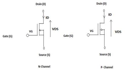
N-Channel MOSFET Operation
In an N-channel MOSFET (NMOS), the substrate is P-type, while the source and drain regions are heavily doped with N-type impurities. When a positive voltage is applied to the gate, it attracts electrons from the substrate towards the gate oxide interface, creating an N-type inversion layer called the channel. This channel allows current to flow between the source and drain when a voltage is applied between them.
P-Channel MOSFET Operation
A P-channel MOSFET (PMOS) works in a similar manner but with opposite polarities. The substrate is N-type, and the source and drain regions are heavily doped with P-type impurities. When a negative voltage is applied to the gate, it attracts holes from the substrate towards the gate oxide interface, creating a P-type inversion layer (channel) that allows current to flow between the source and drain.

Types of MOSFETs
MOSFETs can be classified into several categories based on their structure and operation:
1. Enhancement-Mode MOSFETs
Enhancement-mode MOSFETs are the most common type. They are normally off devices, meaning that there is no conducting channel between the source and drain when the gate voltage is zero. A channel is formed only when the gate voltage exceeds a certain threshold value (Vth).
2. Depletion-Mode MOSFETs
Depletion-mode MOSFETs are normally on devices, meaning that a conducting channel exists between the source and drain even when the gate voltage is zero. To turn off the device, a negative voltage (for N-channel) or a positive voltage (for P-channel) must be applied to the gate.
3. Power MOSFETs
Power MOSFETs are designed to handle high voltages and currents. They have a vertical structure, with the drain and source terminals on opposite sides of the substrate. This allows for better current handling capabilities and lower on-resistance compared to lateral MOSFETs.
| MOSFET Type | Normally On/Off | Gate Voltage to Turn On |
|---|---|---|
| Enhancement-Mode NMOS | Off | Positive |
| Enhancement-Mode PMOS | Off | Negative |
| Depletion-Mode NMOS | On | Negative |
| Depletion-Mode PMOS | On | Positive |

MOSFET Applications
MOSFETs find applications in a wide range of electronic devices and systems:
-
Digital Logic Circuits: MOSFETs are the primary components in digital logic circuits, such as microprocessors, memory devices, and digital signal processors (DSPs).
-
Analog Circuits: MOSFETs are used in analog circuits for signal amplification, switching, and filtering. They are found in operational amplifiers, comparators, and analog-to-digital converters (ADCs).
-
Power Electronics: Power MOSFETs are used in switch-mode power supplies (SMPS), motor drives, and other power conversion applications. They offer high efficiency, fast switching speeds, and low power losses.
-
RF and Microwave Circuits: MOSFETs are used in radio frequency (RF) and microwave circuits for signal amplification and switching. They are found in wireless communication devices, such as smartphones, Wi-Fi routers, and base stations.
-
Automotive Electronics: MOSFETs are used in various automotive electronic systems, such as engine control units (ECUs), power steering, and lighting control.
MOSFET Characteristics and Parameters
When selecting a MOSFET for a specific application, several key characteristics and parameters must be considered:
-
Threshold Voltage (Vth): The minimum gate voltage required to create a conducting channel between the source and drain.
-
On-Resistance (RDS(on)): The resistance between the drain and source when the MOSFET is fully on. A lower RDS(on) results in lower power dissipation and higher efficiency.
-
Breakdown Voltage (BVDSS): The maximum voltage that can be applied between the drain and source without causing avalanche breakdown.
-
Gate Charge (Qg): The amount of charge required to turn the MOSFET on and off. A lower Qg allows for faster switching and lower power consumption.
-
Transconductance (gm): The ratio of the change in drain current to the change in gate voltage. A higher gm indicates a higher gain and faster switching speeds.
MOSFET Fabrication
MOSFETs are fabricated using a series of photolithography, etching, and deposition processes on a semiconductor substrate (usually silicon). The basic steps involved in MOSFET fabrication are:
- Formation of the gate oxide layer
- Deposition and patterning of the gate electrode
- Formation of the source and drain regions through ion implantation or diffusion
- Deposition and patterning of the metal interconnects
Advancements in fabrication technology have led to the development of smaller and more efficient MOSFETs, enabling the creation of highly integrated and complex electronic systems.
MOSFET Scaling and Future Trends
As the demand for faster, smaller, and more power-efficient electronic devices continues to grow, MOSFET scaling has become increasingly important. Scaling refers to the reduction in the physical dimensions of the MOSFET while maintaining or improving its performance.
However, as MOSFETs approach the nanometer scale, several challenges arise, such as increased leakage currents, short-channel effects, and difficulties in fabrication. To overcome these challenges, researchers are exploring new materials, device structures, and fabrication techniques, such as:
- High-k dielectrics for the gate oxide
- Metal gate electrodes
- Multi-gate architectures (e.g., FinFETs, nanowire FETs)
- Strained silicon technology
- III-V compound semiconductors
These advancements aim to extend the scalability of MOSFETs and enable the development of even more advanced electronic devices in the future.
Frequently Asked Questions (FAQ)
-
What is the difference between a MOSFET and a BJT (Bipolar Junction Transistor)?
A MOSFET is a voltage-controlled device, while a BJT is a current-controlled device. MOSFETs have higher input impedance, lower power consumption, and are easier to fabricate compared to BJTs. However, BJTs generally have higher current gain and switching speeds. -
Can a MOSFET be used as a switch?
Yes, MOSFETs are commonly used as switches in electronic circuits. When a MOSFET is fully on, it has a low resistance between the drain and source, allowing current to flow. When it is off, the resistance is very high, blocking the flow of current. -
What is the purpose of the gate oxide in a MOSFET?
The gate oxide is a thin insulating layer that separates the gate electrode from the semiconductor substrate. It allows the gate voltage to control the conductivity of the channel without any direct current flow between the gate and the channel. -
How do enhancement-mode and depletion-mode MOSFETs differ?
Enhancement-mode MOSFETs are normally off devices, meaning they require a gate voltage to create a conducting channel. Depletion-mode MOSFETs are normally on devices, meaning a channel exists even without a gate voltage, and a negative (for N-channel) or positive (for P-channel) gate voltage is required to turn them off. -
What are the advantages of using MOSFETs in power electronics applications?
MOSFETs offer several advantages in power electronics applications, such as high efficiency, fast switching speeds, and low power losses. They also have a higher input impedance and are easier to drive compared to other power semiconductor devices like IGBTs (Insulated Gate Bipolar Transistors) and thyristors.
Conclusion
MOSFETs are essential components in modern electronics, serving as the building blocks for a wide range of devices and systems. By understanding the basic structure, operation, and types of MOSFETs, engineers and enthusiasts can better appreciate their role in shaping the electronic landscape.
As technology continues to advance, MOSFETs will likely remain at the forefront of innovation, with ongoing research and development focused on improving their performance, efficiency, and scalability. By staying informed about the latest trends and advancements in MOSFET technology, one can gain a deeper understanding of the future of electronics and the countless possibilities it holds.


Leave a Reply