Introduction to PCB Phototools
Printed Circuit Board (PCB) fabrication is a complex process that involves several steps, including PCB design, PCB Prototyping, and PCB manufacturing. One of the critical stages in this process is the image transfer of the PCB design onto the copper-clad board. This is where PCB phototools come into play.
PCB phototools are high-resolution films or glass masks used to transfer the PCB design onto the copper-clad board using a photoresist process. They are an essential component in the PCB manufacturing process as they ensure the accurate and precise transfer of the PCB design onto the board.
Types of PCB Phototools
There are two main types of PCB phototools:
- Film Phototools
- Glass Phototools
Film Phototools
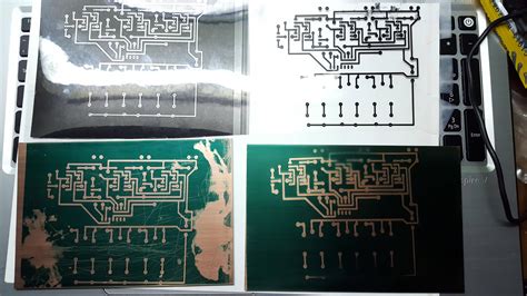
Film phototools are the most common type of PCB phototools. They are made of a clear polyester film with a photosensitive emulsion layer on one side. The PCB design is printed onto the film using a high-resolution printer, creating a negative image of the PCB design.
Film phototools are relatively inexpensive and easy to produce. They are suitable for low-volume production runs and prototyping. However, they have some limitations, such as lower resolution compared to glass phototools and a shorter lifespan.
Glass Phototools
Glass phototools are high-end PCB phototools that offer superior resolution and accuracy compared to film phototools. They are made of a glass substrate with a chrome layer on one side. The PCB design is etched onto the chrome layer using a laser or e-beam writer, creating a positive image of the PCB design.
Glass phototools are more expensive than film phototools and are typically used for high-volume production runs and high-density PCB designs. They offer several advantages over film phototools, such as:
- Higher resolution (up to 50,000 dpi)
- Better dimensional stability
- Longer lifespan
- Improved registration accuracy
PCB Phototool Specifications
When choosing PCB phototools, several specifications need to be considered to ensure the best results. These include:
- Resolution
- Minimum feature size
- Registration accuracy
- Dimensional stability
- Optical density
Resolution
Resolution refers to the level of detail that can be achieved in the PCB design. It is measured in dots per inch (dpi) or microns (μm). The higher the resolution, the finer the details that can be printed on the PCB.
| Phototool Type | Resolution Range |
|---|---|
| Film Phototools | 4,000 – 16,000 dpi |
| Glass Phototools | 20,000 – 50,000 dpi |
Minimum Feature Size
Minimum feature size refers to the smallest feature that can be reliably printed on the PCB. It is measured in microns (μm) and is determined by the resolution of the phototool and the capabilities of the PCB manufacturing process.
| Phototool Type | Minimum Feature Size |
|---|---|
| Film Phototools | 50 – 100 μm |
| Glass Phototools | 25 – 50 μm |
Registration Accuracy
Registration accuracy refers to the ability to align multiple layers of the PCB design accurately. It is critical for multi-layer PCBs and is measured in microns (μm).
| Phototool Type | Registration Accuracy |
|---|---|
| Film Phototools | ± 50 – 100 μm |
| Glass Phototools | ± 10 – 25 μm |
Dimensional Stability
Dimensional stability refers to the ability of the phototool to maintain its size and shape over time and under varying environmental conditions. It is critical for maintaining the accuracy of the PCB design and is measured in parts per million (ppm).
| Phototool Type | Dimensional Stability |
|---|---|
| Film Phototools | 100 – 500 ppm |
| Glass Phototools | 10 – 50 ppm |
Optical Density
Optical density refers to the ability of the phototool to block light in the non-image areas. It is critical for achieving a clean and sharp image transfer onto the PCB. The higher the optical density, the better the contrast between the image and non-image areas.
| Phototool Type | Optical Density |
|---|---|
| Film Phototools | 3.0 – 4.0 |
| Glass Phototools | 4.0 – 5.0 |
PCB Phototool Manufacturing Process
The PCB phototool manufacturing process involves several steps, including:
- PCB Design
- Phototool Preparation
- Exposure
- Development
- Etching
- Stripping
- Inspection
PCB Design
The first step in the PCB phototool manufacturing process is the PCB design. The PCB design is created using specialized software, such as Altium Designer or Eagle. The design includes all the necessary components, such as traces, pads, and vias.
Phototool Preparation
Once the PCB design is complete, it is sent to a phototool manufacturer for preparation. The phototool manufacturer will review the design files to ensure they meet the required specifications, such as resolution, minimum feature size, and registration accuracy.
For film phototools, the design is printed onto a clear polyester film using a high-resolution printer. The printer uses a special ink that is opaque to UV light, creating a negative image of the PCB design.
For glass phototools, the design is etched onto a chrome-coated glass substrate using a laser or e-beam writer. The laser or e-beam writer removes the chrome in the non-image areas, creating a positive image of the PCB design.
Exposure
Once the phototool is prepared, it is used to expose the photoresist-coated copper-clad board. The board is placed in contact with the phototool and exposed to UV light. The UV light passes through the clear areas of the phototool and hardens the photoresist in those areas.
Development
After exposure, the board is developed using a chemical solution that removes the unhardened photoresist. This leaves a positive image of the PCB design on the copper-clad board.
Etching
The next step is to etch away the unwanted copper from the board using a chemical solution, such as ferric chloride or ammonium persulfate. The hardened photoresist acts as a protective layer, preventing the copper underneath from being etched away.
Stripping
After etching, the remaining photoresist is stripped away using a chemical solution, leaving the final PCB design on the copper-clad board.
Inspection
The final step in the PCB phototool manufacturing process is inspection. The PCB is inspected for any defects, such as shorts, opens, or misalignments. If any defects are found, the board is reworked or scrapped.

Benefits of Using PCB Phototools
Using PCB phototools offers several benefits, including:
- High Accuracy
- Improved Productivity
- Cost-Effectiveness
- Consistency
High Accuracy
PCB phototools offer high accuracy and precision in transferring the PCB design onto the copper-clad board. This is especially important for high-density PCB designs with small features and tight tolerances.
Improved Productivity
Using PCB phototools can significantly improve productivity in the PCB manufacturing process. Phototools allow for the rapid and accurate transfer of the PCB design onto multiple boards simultaneously, reducing the overall manufacturing time.
Cost-Effectiveness
PCB phototools are cost-effective for high-volume production runs. Although the initial cost of producing a phototool may be higher than other methods, such as direct printing or milling, the cost per board is significantly lower when produced in large quantities.
Consistency
PCB phototools provide consistent results across multiple production runs. This is because the phototool is a fixed image of the PCB design and does not vary from one board to another, ensuring that each board is identical to the original design.

Challenges and Limitations of PCB Phototools
Despite the many benefits of using PCB phototools, there are also some challenges and limitations to consider, including:
- Initial Cost
- Limited Flexibility
- Phototool Degradation
Initial Cost
The initial cost of producing a PCB phototool can be high, especially for glass phototools. This can be a significant barrier for low-volume production runs or prototyping.
Limited Flexibility
PCB phototools are a fixed image of the PCB design and cannot be easily modified once produced. This can be a limitation when design changes are required, as a new phototool must be produced for each revision.
Phototool Degradation
PCB phototools can degrade over time due to exposure to UV light, humidity, and handling. This can lead to reduced accuracy and quality in the PCB manufacturing process.

Conclusion
PCB phototools are an essential component in the PCB manufacturing process, providing high accuracy, improved productivity, cost-effectiveness, and consistency. When choosing PCB phototools, it is important to consider the specifications, such as resolution, minimum feature size, registration accuracy, dimensional stability, and optical density, to ensure the best results for your specific PCB design.
While there are some challenges and limitations to using PCB phototools, such as initial cost, limited flexibility, and phototool degradation, the benefits far outweigh the drawbacks for most PCB manufacturing applications.
Frequently Asked Questions (FAQ)
-
What is the difference between film and glass phototools?
Film phototools are made of a clear polyester film with a photosensitive emulsion layer and are suitable for low-volume production runs and prototyping. Glass phototools are made of a glass substrate with a chrome layer and offer superior resolution and accuracy, making them ideal for high-volume production runs and high-density PCB designs. -
What is the minimum feature size that can be achieved with PCB phototools?
The minimum feature size that can be achieved with PCB phototools depends on the type of phototool used. Film phototools can achieve a minimum feature size of 50-100 μm, while glass phototools can achieve a minimum feature size of 25-50 μm. -
How does the resolution of PCB phototools affect the PCB design?
The resolution of PCB phototools determines the level of detail that can be achieved in the PCB design. Higher resolution phototools can produce finer details and smaller features, which is important for high-density PCB designs. -
What is the typical lifespan of PCB phototools?
The lifespan of PCB phototools depends on several factors, such as handling, storage, and exposure to UV light and humidity. Film phototools typically have a shorter lifespan compared to glass phototools, which can last for several years with proper care and storage. -
Can PCB phototools be modified once they are produced?
PCB phototools are a fixed image of the PCB design and cannot be easily modified once produced. If design changes are required, a new phototool must be produced for each revision.


Leave a Reply