Understanding the Importance of PCB-DFM in Electronics Manufacturing
In the world of electronics manufacturing, the process of designing and fabricating printed circuit boards (PCBs) is a critical step. PCBs are the backbone of almost all electronic devices, connecting and supporting various components to ensure proper functionality. To guarantee the successful production of PCBs, it is essential to consider Design for Manufacturability (DFM) principles. DFM is a methodology that optimizes the design of a product to ensure efficient and cost-effective manufacturing. In the context of PCBs, DFM focuses on creating designs that are compatible with the manufacturing processes, materials, and equipment used in PCB fabrication.
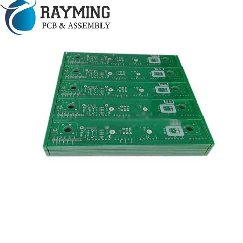
One of the key aspects of PCB-DFM is the generation and management of production data, which includes Gerber files. Gerber files are the industry standard for conveying PCB design information to manufacturing facilities. They contain critical data about the PCB layout, including the copper layers, solder mask, silkscreen, and drill holes. Proper creation and handling of Gerber files is essential to ensure that the manufactured PCB meets the designer’s intent and functions as expected.
In this article, we will explore the process of transforming Gerber files into PCB production data, focusing on the principles of PCB-DFM. We will discuss the various steps involved, the tools and techniques used, and the best practices for ensuring a smooth transition from design to manufacturing. By understanding the importance of PCB-DFM and implementing the appropriate measures, designers and manufacturers can collaborate effectively to produce high-quality, reliable PCBs.
The Role of Gerber Files in PCB Manufacturing
Gerber files are named after the Gerber Scientific Instrument Company, which developed the Gerber format in the 1960s. The Gerber format has since become the de facto standard for exchanging PCB design information between designers and manufacturers. Gerber files are ASCII text files that contain a series of commands and coordinates that describe the various layers and features of a PCB.
A typical set of Gerber files for a PCB includes:
- Copper layers (e.g., top and bottom)
- Solder mask layers
- Silkscreen layers
- Solder paste layers
- Drill files (for the location and size of holes)
Each Gerber file represents a specific layer or aspect of the PCB design. The files use a coordinate system to define the location and shape of traces, pads, and other features. Manufacturers use specialized software to interpret these files and generate the necessary tooling and machining instructions for fabricating the PCB.
| File Extension | Layer Description |
|---|---|
| .GTL | Top Copper Layer |
| .GBL | Bottom Copper Layer |
| .GTS | Top Solder Mask Layer |
| .GBS | Bottom Solder Mask Layer |
| .GTO | Top Silkscreen Layer |
| .GBO | Bottom Silkscreen Layer |
| .GTP | Top Paste Mask Layer |
| .GBP | Bottom Paste Mask Layer |
| .DRL | Drill File |
It is essential for designers to generate accurate and complete Gerber files to ensure that the manufactured PCB matches the intended design. Inconsistencies or errors in Gerber files can lead to manufacturing defects, delays, and increased costs.

Preparing Gerber Files for Manufacturing
To ensure a smooth transition from PCB design to manufacturing, designers must prepare Gerber files that adhere to PCB-DFM principles. This involves following best practices and guidelines that optimize the design for manufacturability. Some key considerations when preparing Gerber files include:
1. Ensure Gerber File Completeness
A complete set of Gerber files should include all the necessary layers and information required for manufacturing. This includes copper layers, solder mask, silkscreen, drill files, and any additional files specified by the manufacturer. Incomplete or missing files can lead to delays and confusion during the manufacturing process.
2. Use Standard Gerber Format
Designers should use the standard Gerber format (RS-274X) when generating files. This format is widely accepted by PCB manufacturers and ensures compatibility with their software and equipment. Using non-standard or proprietary formats can lead to issues during file interpretation and processing.
3. Adhere to Manufacturer’s Specifications
Each PCB manufacturer may have specific requirements and guidelines for Gerber files. These can include naming conventions, file extensions, layer stack-up information, and minimum feature sizes. Designers should obtain and follow the manufacturer’s specifications to ensure compliance and avoid potential issues.
4. Perform Design Rule Checks (DRC)
Before generating Gerber files, designers should perform thorough Design Rule Checks (DRC) on their PCB layout. DRC helps identify and resolve design issues, such as trace width violations, clearance errors, and manufacturing constraints. Conducting DRC ensures that the design is manufacturable and reduces the risk of defects and delays.
5. Include Necessary Annotations and Notes
Gerber files should include relevant annotations and notes that provide additional information to the manufacturer. This can include layer stack-up details, material specifications, finish requirements, and any special instructions. Clear communication through annotations helps avoid misinterpretations and ensures that the manufacturer has all the necessary information to produce the PCB correctly.

Gerber File Analysis and Optimization
Once the Gerber files are generated, they undergo analysis and optimization to ensure compatibility with the manufacturing processes and to identify potential issues. This step is crucial in the PCB-DFM workflow, as it helps detect and resolve design problems before they impact the manufacturing stage. Some common analyses and optimizations performed on Gerber files include:
1. Design Rule Checking (DRC)
Manufacturers often perform their own DRC on the received Gerber files to verify compliance with their manufacturing capabilities and constraints. This additional check helps catch any design issues that may have been missed during the designer’s DRC process. Manufacturers use specialized software to analyze the Gerber files and generate DRC reports, highlighting any violations or areas of concern.
2. Panelization
PCB Panelization is the process of arranging multiple PCB designs on a single panel for efficient manufacturing. Manufacturers analyze the Gerber files to determine the optimal panel layout, considering factors such as PCB dimensions, spacing, and tooling requirements. Panelization helps maximize material utilization, reduce production time, and lower manufacturing costs.
3. Gerber File Optimization
Manufacturers may optimize the Gerber files to enhance manufacturability and improve efficiency. This can include adjusting trace widths, pad sizes, and clearances to match their manufacturing capabilities. They may also modify the Gerber files to accommodate specific tooling or processes, such as adding fiducial marks or optimizing the drill file for their drilling equipment.
4. Netlist Comparison
In some cases, manufacturers may request the PCB netlist in addition to the Gerber files. The netlist contains information about the electrical connections between components on the PCB. Manufacturers can compare the netlist with the Gerber files to verify the integrity of the design and ensure that all connections are accurately represented. This helps catch any discrepancies between the schematic and the PCB layout.

Generating PCB Production Data
After the Gerber files have been analyzed and optimized, the next step is to generate the PCB production data. This data includes the specific instructions and files needed to fabricate the PCB. The production data is typically generated using Computer-Aided Manufacturing (CAM) software, which processes the Gerber files and creates the necessary toolpaths and machine instructions.
Some key elements of PCB production data include:
-
Drill Files: The drill files contain information about the location, size, and type of holes to be drilled in the PCB. This data is used to program the drilling equipment and ensure accurate hole placement.
-
Solder Mask and Silkscreen Data: The CAM software generates the data needed to apply the solder mask and silkscreen layers to the PCB. This includes the necessary artwork and positioning information for these layers.
-
Copper Layer Data: The production data includes the toolpaths and instructions for creating the copper traces and pads on each layer of the PCB. This data guides the etching or plating processes used to form the conductive patterns.
-
Inspection Data: CAM software can generate data for automated optical inspection (AOI) or other quality control processes. This data helps verify the accuracy and integrity of the manufactured PCB.
The generated production data is then used to program and control the various machines and equipment involved in the PCB fabrication process. This includes drilling machines, etching equipment, plating systems, and inspection tools. By using precise and optimized production data, manufacturers can ensure high-quality and consistent PCB production.
Best Practices for PCB-DFM
To optimize the PCB design and manufacturing process, designers and manufacturers should follow best practices for PCB-DFM. These practices help minimize errors, improve efficiency, and ensure the successful production of reliable PCBs. Some key best practices include:
-
Early Collaboration: Designers should engage with manufacturers early in the design process to discuss DFM requirements and constraints. Early collaboration helps identify potential issues and allows for proactive design adjustments.
-
Adherence to Design Guidelines: Designers should follow industry-standard design guidelines and the manufacturer’s specific requirements. This includes adhering to minimum trace widths, clearances, drill sizes, and other design rules.
-
Clear Communication: Effective communication between designers and manufacturers is essential. Designers should provide clear and complete documentation, including Gerber files, BOM, and assembly instructions. Manufacturers should offer feedback and guidance on DFM considerations.
-
Design Review and Verification: Conducting thorough design reviews and verifications helps catch potential issues early in the process. This includes performing DRC, netlist comparisons, and manufacturability assessments.
-
Continuous Improvement: Designers and manufacturers should continuously monitor and analyze the PCB design and manufacturing process to identify areas for improvement. This can involve collecting data, conducting root cause analyses, and implementing corrective actions to enhance quality and efficiency.
By following these best practices and collaborating effectively, designers and manufacturers can streamline the PCB-DFM process, reduce errors and delays, and produce high-quality PCBs that meet the required specifications.
Frequently Asked Questions (FAQ)
-
Q: What are Gerber files, and why are they important in PCB manufacturing?
A: Gerber files are the industry standard for conveying PCB design information to manufacturing facilities. They contain critical data about the PCB layout, including copper layers, solder mask, silkscreen, and drill holes. Gerber files are essential for accurately communicating the designer’s intent to the manufacturer and ensuring the proper fabrication of the PCB. -
Q: What is PCB-DFM, and how does it impact the manufacturing process?
A: PCB-DFM (Design for Manufacturability) is a methodology that optimizes the design of a PCB to ensure efficient and cost-effective manufacturing. It involves considering the manufacturing processes, materials, and equipment during the design phase to minimize potential issues and improve the overall quality and reliability of the manufactured PCB. PCB-DFM helps reduce errors, delays, and costs in the manufacturing process. -
Q: What are some common issues that can arise from poorly prepared Gerber files?
A: Poorly prepared Gerber files can lead to various manufacturing issues, such as incorrect layer alignment, missing or incomplete data, and violations of design rules. These issues can result in manufacturing defects, delays, and increased costs. It is crucial for designers to generate accurate and complete Gerber files that adhere to PCB-DFM principles to avoid these problems. -
Q: How can designers and manufacturers collaborate effectively to ensure successful PCB production?
A: Effective collaboration between designers and manufacturers involves early communication, adherence to design guidelines, clear documentation, and continuous improvement. Designers should engage with manufacturers early in the design process to discuss DFM requirements and constraints. They should follow industry-standard design guidelines and provide clear and complete documentation, including Gerber files and assembly instructions. Manufacturers should offer feedback and guidance on DFM considerations. Both parties should work together to monitor and improve the PCB design and manufacturing process continuously. -
Q: What role does CAM software play in generating PCB production data?
A: CAM (Computer-Aided Manufacturing) software plays a crucial role in generating PCB production data. It processes the Gerber files and creates the necessary toolpaths and machine instructions for fabricating the PCB. CAM software generates data for drilling, solder mask and silkscreen application, copper layer etching or plating, and inspection processes. The generated production data is used to program and control the various machines and equipment involved in the PCB fabrication process, ensuring accurate and consistent production.
Conclusion
In conclusion, the process of transforming Gerber files into PCB production data is a critical step in the electronics manufacturing workflow. By understanding the principles of PCB-DFM and implementing best practices, designers and manufacturers can collaborate effectively to ensure the successful production of high-quality and reliable PCBs.
Gerber files serve as the essential link between PCB design and manufacturing, containing the necessary information for fabricating the PCB. Proper preparation and handling of Gerber files, along with adherence to DFM guidelines, help minimize errors and optimize the manufacturing process.
Through Gerber file analysis, optimization, and the generation of precise production data, manufacturers can streamline the PCB fabrication process and produce PCBs that meet the required specifications. Continuous collaboration, communication, and improvement between designers and manufacturers are key to achieving successful PCB production.
By prioritizing PCB-DFM and following industry best practices, companies can enhance the efficiency, quality, and cost-effectiveness of their PCB manufacturing operations. This ultimately leads to the development of better electronic products and the advancement of the electronics industry as a whole.


Leave a Reply