What is PCB Assembly?
PCB assembly is the process of soldering or mounting electronic components onto a printed circuit board (PCB). It is a crucial step in the manufacturing of electronic devices, as it involves attaching various components such as resistors, capacitors, integrated circuits, and connectors to the PCB. The assembled PCB then functions as the backbone of the electronic device, enabling it to perform its intended tasks.
PCB assembly can be carried out through various methods, depending on the complexity of the board and the volume of production. The two main types of PCB assembly are:
- Through-hole assembly (THA)
- Surface mount assembly (SMA)
Through-hole Assembly (THA)
Through-hole assembly involves inserting component leads through drilled holes in the PCB and soldering them to pads on the opposite side of the board. This method is typically used for larger components or when mechanical strength is a priority. The process can be carried out manually or using automated machines.
Advantages of through-hole assembly:
– Stronger mechanical bonds
– Easier to replace or repair components
– Suitable for high-power applications
Disadvantages of through-hole assembly:
– Larger component size
– Increased board space requirements
– Slower assembly process compared to surface mount technology
Surface Mount Assembly (SMA)
Surface mount assembly involves placing components directly onto pads on the surface of the PCB and soldering them in place. This method allows for smaller components and higher density layouts, making it the preferred choice for most modern electronic devices. Surface mount assembly is typically carried out using automated pick-and-place machines and reflow soldering processes.
Advantages of surface mount assembly:
– Smaller component size
– Higher component density
– Faster assembly process
– Lower production costs
Disadvantages of surface mount assembly:
– Difficulty in manual assembly and repairs
– Requires specialized equipment for assembly
– More susceptible to thermal stress and vibration
PCB Assembly Process
The PCB assembly process consists of several steps, each of which must be carried out with precision to ensure the quality and reliability of the final product. The main steps involved in PCB assembly are:
- Solder paste application
- Component placement
- Reflow soldering
- Inspection and testing
Solder Paste Application
Solder paste, a mixture of tiny solder particles suspended in a flux medium, is applied to the PCB pads using a stencil or screen printing process. The stencil is a thin metal sheet with apertures that correspond to the PCB pads. The solder paste is spread over the stencil, filling the apertures and depositing the paste onto the pads when the stencil is removed.
Component Placement
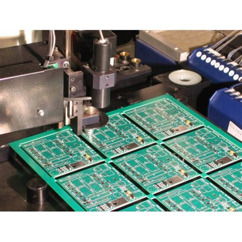
After solder paste application, the components are placed onto their respective pads on the PCB. For through-hole assembly, the components are inserted manually or using automated insertion machines. In surface mount assembly, automated pick-and-place machines are used to rapidly place components onto the PCB with high precision.
Reflow Soldering
Once the components are placed, the PCB undergoes a reflow soldering process. The board is heated in a reflow oven, causing the solder paste to melt and form a permanent connection between the components and the PCB pads. The reflow soldering process typically follows a temperature profile that gradually heats the board, maintains a peak temperature for a specified duration, and then cools it down.
Inspection and Testing
After the reflow soldering process, the assembled PCB undergoes various inspection and testing procedures to ensure its quality and functionality. These may include:
- Visual inspection: Checking for proper component placement, solder joint quality, and any visible defects.
- Automated optical inspection (AOI): Using cameras and image processing software to detect assembly defects.
- X-ray inspection: Examining solder joints and internal connections that are not visible from the surface.
- In-circuit testing (ICT): Verifying the functionality of individual components and their interconnections.
- Functional testing: Ensuring that the assembled PCB performs its intended functions as part of the final product.

PCB Assembly Services
Given the complexity and precision required for PCB assembly, many companies opt to outsource this process to specialized PCB assembly service providers. These providers offer a range of services, from prototyping to high-volume production, and cater to various industries, such as consumer electronics, automotive, medical devices, and aerospace.
When choosing a PCB assembly service provider, consider the following factors:
-
Technical capabilities: Ensure that the provider has the necessary equipment, expertise, and certifications to handle your specific PCB assembly requirements.
-
Quality control: Look for providers with robust quality control processes, such as ISO 9001 certification, and a track record of delivering high-quality assembled PCBs.
-
Turnaround time: Consider the provider’s ability to meet your project deadlines, especially for time-sensitive applications.
-
Cost: Compare pricing among different providers, but keep in mind that the lowest cost option may not always be the best choice when factoring in quality and reliability.
-
Customer support: Choose a provider that offers responsive and knowledgeable customer support to help address any issues or concerns throughout the assembly process.
| Service Provider | Capabilities | Certifications | Turnaround Time | Price Range |
|---|---|---|---|---|
| PCB Proto | Prototyping, low-volume | ISO 9001 | 5-10 days | $ |
| ABC Assembly | High-volume, automotive | IATF 16949 | 2-4 weeks | $$ |
| XYZ Electronics | Medical devices, aerospace | ISO 13485, AS9100 | 3-6 weeks | $$$ |
| Acme PCB | Consumer electronics, IoT | ISO 9001 | 1-3 weeks | $$ |
*Note: Price range is indicative and may vary based on specific project requirements.

Benefits of Outsourcing PCB Assembly
Outsourcing PCB assembly to a specialized service provider offers several benefits, including:
-
Cost savings: Outsourcing eliminates the need to invest in expensive assembly equipment and maintain a skilled workforce, reducing overall production costs.
-
Expertise: PCB assembly service providers have the knowledge and experience to handle complex assemblies and ensure high-quality results.
-
Scalability: Service providers can accommodate varying production volumes, from prototypes to high-volume runs, allowing companies to scale their production as needed.
-
Time savings: By outsourcing PCB assembly, companies can focus on their core competencies and product development, while the assembly process is handled by the service provider.
-
Access to advanced technologies: PCB assembly service providers invest in the latest equipment and technologies to stay competitive, enabling companies to benefit from these advancements without direct investment.

Choosing the Right PCB Assembly Partner
When selecting a PCB assembly partner, it is essential to consider their capabilities, quality control processes, and customer support. PCB Proto, a leading provider of PCB assembly services, offers a comprehensive range of solutions for prototyping and low-volume production.
PCB Proto’s key advantages include:
- ISO 9001 certified quality management system
- Experienced team of assembly technicians
- State-of-the-art assembly equipment
- Rapid prototyping capabilities
- Competitive pricing
- Responsive customer support
By partnering with PCB Proto, companies can benefit from high-quality PCB assembly services that meet their specific requirements and help bring their electronic products to market faster and more efficiently.
Conclusion
PCB assembly is a critical process in the production of electronic devices, requiring precision, expertise, and advanced technologies. Outsourcing PCB assembly to a specialized service provider like PCB Proto offers numerous benefits, including cost savings, access to expertise, scalability, and time savings. By carefully considering the capabilities, quality control processes, and customer support of potential PCB assembly partners, companies can ensure the success of their electronic products in today’s competitive market.
Frequently Asked Questions (FAQ)
1. What is the minimum order quantity for PCB assembly at PCB Proto?
PCB Proto specializes in prototyping and low-volume production, with a minimum order quantity of 1 PCB. This allows companies to quickly test and validate their designs before committing to larger production runs.
2. How long does PCB assembly take at PCB Proto?
The turnaround time for PCB assembly at PCB Proto typically ranges from 5 to 10 days, depending on the complexity of the assembly and the current workload. Rush services may be available for time-sensitive projects.
3. What file formats are required for PCB assembly?
To begin the PCB assembly process, PCB Proto requires the following files:
- Gerber files (RS-274X format)
- Bill of Materials (BOM)
- Pick and Place file (Centroid or XY data)
- Assembly drawings or instructions (if applicable)
4. Does PCB Proto offer design review services?
Yes, PCB Proto offers design review services to help identify potential issues or improvements before the assembly process begins. This can help save time and costs by catching problems early in the development cycle.
5. What certifications does PCB Proto hold?
PCB Proto is ISO 9001 certified, demonstrating its commitment to quality management and continuous improvement in its PCB assembly processes. This certification ensures that customers can rely on PCB Proto to deliver consistently high-quality assembled PCBs.


Leave a Reply