Table of Contents
- PCBs”>Introduction to PCBs
- PCB Structure and Components
- Types of PCBs
- Single-Sided PCBs
- Double-sided PCBs
- Multi-layer PCBs
- Flexible PCBs
- Rigid-flex PCBs
- PCB Manufacturing Process
- Design and Layout
- Printing and Etching
- Drilling and Plating
- Solder Mask and Silkscreen
- Surface Finish
- Quality Control and Testing
- PCB Materials
- Substrate Materials
- Copper Foil
- Solder Mask
- Silkscreen
- PCB Design Considerations
- Component Placement
- Trace Routing
- Power and Ground Planes
- Signal Integrity
- Electromagnetic Compatibility
- PCB Testing and Inspection
- Visual Inspection
- Automated Optical Inspection (AOI)
- In-Circuit Testing (ICT)
- Functional Testing
- PCB Assembly
- Through-Hole Assembly
- Surface Mount Assembly
- Mixed Technology Assembly
- PCB Applications
- Consumer Electronics
- Automotive Industry
- Medical Devices
- Aerospace and Defense
- Industrial Automation
- Future Trends in PCB Technology
- Frequently Asked Questions (FAQ)
- Conclusion
Introduction to PCBs
A Printed Circuit Board (PCB) is a thin board made of fiberglass or other composite materials, with conductive pathways etched or printed onto its surface. These pathways, known as traces, connect various electronic components such as resistors, capacitors, and integrated circuits (ICs) to form a functional electronic circuit.
PCBs have become an essential part of modern electronics due to their numerous advantages over traditional point-to-point wiring:
- Compact size: PCBs allow for the miniaturization of electronic devices by providing a compact and efficient way to interconnect components.
- Reliability: The use of PCBs reduces the risk of loose connections and short circuits, resulting in more reliable electronic devices.
- Mass production: PCBs can be easily mass-produced using automated manufacturing processes, reducing costs and increasing production efficiency.
- Consistency: PCBs ensure consistent electrical characteristics and performance across multiple units of the same design.

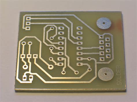
PCB Structure and Components
A typical PCB consists of several layers, each serving a specific purpose:
- Substrate: The substrate is the base material of the PCB, typically made of fiberglass or other composite materials. It provides mechanical support and electrical insulation between the conductive layers.
- Copper layers: Thin sheets of copper foil are laminated onto the substrate to create the conductive pathways for electrical signals. The number of copper layers depends on the complexity of the circuit and the PCB type.
- Solder mask: A thin layer of polymer is applied over the copper traces to protect them from oxidation and prevent accidental short circuits during soldering. The solder mask is typically green, but other colors are also available.
- Silkscreen: A layer of text and symbols is printed onto the PCB surface to provide information about component placement, orientation, and identification. The silkscreen is typically white, but other colors can be used for better contrast or aesthetics.
- Vias: Vias are small holes drilled through the PCB to interconnect traces on different layers. They can be filled with conductive material (plated through-holes) or left open (non-plated through-holes).
In addition to these structural elements, PCBs also contain various electronic components that are mounted onto the board using soldering techniques. These components include:
- Resistors
- Capacitors
- Inductors
- Diodes
- Transistors
- Integrated Circuits (ICs)
- Connectors
- Switches
- LEDs
- and more
The specific components used in a PCB depend on the intended function and application of the electronic device.

Types of PCBs
There are several types of PCBs, each with its own unique characteristics and applications. The most common types include:
Single-sided PCBs
Single-sided PCBs have conductive traces on only one side of the substrate. They are the simplest and most cost-effective type of PCB, suitable for basic electronic circuits with low component density. Single-sided PCBs are commonly used in low-cost consumer electronics, such as toys and simple appliances.
Double-sided PCBs
Double-sided PCBs have conductive traces on both sides of the substrate, allowing for higher component density and more complex circuits compared to single-sided PCBs. The two layers are interconnected using vias. Double-sided PCBs are used in a wide range of applications, including computers, televisions, and automotive electronics.
Multi-layer PCBs
Multi-layer PCBs consist of three or more conductive layers, separated by insulating layers. They offer the highest component density and are used in complex electronic devices that require a large number of interconnections, such as smartphones, laptops, and medical equipment. Multi-layer PCBs can have up to 50 layers or more, depending on the application.
Flexible PCBs
Flexible PCBs, also known as flex circuits, are made using flexible substrate materials, such as polyimide or polyester. They can bend and conform to various shapes, making them ideal for applications that require flexibility or space-saving designs. Flexible PCBs are commonly used in wearable electronics, medical devices, and aerospace applications.
Rigid-Flex PCBs
Rigid-Flex PCBs combine the benefits of both rigid and flexible PCBs. They consist of rigid PCB sections connected by flexible PCB sections, allowing for three-dimensional packaging and improved reliability in applications that require both stability and flexibility. Rigid-Flex PCBs are used in complex electronic devices, such as smartphones, tablets, and military equipment.

PCB Manufacturing Process
The PCB manufacturing process involves several steps, each critical to ensuring the quality and reliability of the final product. The main stages of PCB fabrication include:
Design and Layout
The PCB manufacturing process begins with the creation of a schematic diagram and a PCB layout using computer-aided design (CAD) software. The schematic diagram represents the electrical connections between components, while the PCB layout determines the physical placement of components and routing of traces on the board.
Printing and Etching
Once the design is finalized, the PCB layout is printed onto the copper-clad substrate using a photoresist process. The exposed areas of the photoresist are then developed and removed, leaving behind a pattern of the desired traces. The unwanted copper is etched away using a chemical solution, leaving only the desired conductive traces on the substrate.
Drilling and Plating
After etching, holes are drilled into the PCB to accommodate through-hole components and vias. The holes are then plated with a conductive material, typically copper, to ensure electrical connectivity between layers.
Solder Mask and Silkscreen
A solder mask is applied to the PCB surface to protect the copper traces from oxidation and prevent accidental short circuits during soldering. The silkscreen layer is then added to provide text and symbols for component placement and identification.
Surface Finish
The exposed copper areas of the PCB, such as pads and plated through-holes, are coated with a protective surface finish to prevent oxidation and improve solderability. Common surface finishes include Hot Air Solder Leveling (HASL), Electroless Nickel Immersion Gold (ENIG), and Immersion Silver.
Quality Control and Testing
Throughout the manufacturing process, various quality control measures are implemented to ensure the PCBs meet the required specifications. These measures include visual inspections, automated optical inspection (AOI), and electrical testing.
PCB Materials
The choice of materials used in PCB fabrication plays a crucial role in determining the performance, reliability, and cost of the final product. The main materials used in PCBs include:
Substrate Materials
The most common substrate material for PCBs is FR-4, a fiberglass-reinforced epoxy laminate. Other substrate materials include:
- Polyimide: Used for flexible PCBs and high-temperature applications
- Ceramic: Used for high-frequency and high-power applications
- Aluminum: Used for heat dissipation in power electronics
Copper Foil
Copper foil is used to create the conductive traces on the PCB. The thickness of the copper foil is typically measured in ounces per square foot (oz/ft²), with common thicknesses ranging from 0.5 oz/ft² to 2 oz/ft².
Solder Mask
The solder mask is a thin layer of polymer applied over the copper traces to protect them from oxidation and prevent accidental short circuits during soldering. Solder masks are available in various colors, with green being the most common.
Silkscreen
The silkscreen is a layer of text and symbols printed onto the PCB surface to provide information about component placement, orientation, and identification. The silkscreen is typically white, but other colors can be used for better contrast or aesthetics.
PCB Design Considerations
Designing a high-quality PCB requires careful consideration of several factors to ensure optimal performance, reliability, and manufacturability. Some key design considerations include:
Component Placement
Components should be placed on the PCB in a way that minimizes the length of traces, reduces electromagnetic interference (EMI), and facilitates easy assembly and maintenance.
Trace Routing
Traces should be routed in a manner that minimizes crosstalk, signal reflections, and electromagnetic compatibility (EMC) issues. Proper trace width and spacing should be maintained based on the signal characteristics and PCB manufacturing capabilities.
Power and Ground Planes
Dedicated power and ground planes should be used to distribute power evenly across the PCB and minimize voltage drops. Proper decoupling and filtering techniques should be employed to reduce noise and ensure signal integrity.
Signal Integrity
High-speed digital signals require careful design considerations to maintain signal integrity. Techniques such as impedance matching, termination, and differential signaling should be used to minimize signal distortion and ensure reliable data transmission.
Electromagnetic Compatibility
PCBs should be designed to minimize electromagnetic interference (EMI) and ensure compliance with relevant EMC standards. Proper grounding, shielding, and filtering techniques should be employed to reduce electromagnetic emissions and susceptibility.
PCB Testing and Inspection
To ensure the quality and reliability of PCBs, various testing and inspection methods are employed during and after the manufacturing process. Some common techniques include:
Visual Inspection
Visual inspection is the most basic form of PCB testing, where the board is examined for obvious defects such as missing components, incorrect component placement, or solder bridging.
Automated Optical Inspection (AOI)
AOI uses high-resolution cameras and image processing software to automatically detect manufacturing defects such as missing components, incorrect component placement, and solder bridging.
In-Circuit Testing (ICT)
ICT involves using a bed-of-nails fixture to make electrical contact with specific points on the PCB and verify the presence, orientation, and functionality of components.
Functional Testing
Functional testing involves powering up the PCB and verifying that it performs its intended function according to the design specifications. This can include testing the board’s response to various input signals and measuring output signals.
PCB Assembly
PCB assembly is the process of populating the PCB with electronic components and soldering them in place. There are three main types of PCB assembly:
Through-Hole Assembly
Through-hole assembly involves inserting component leads through drilled holes in the PCB and soldering them to pads on the opposite side. This assembly method is suitable for larger components and provides strong mechanical connections.
Surface Mount Assembly
Surface mount assembly involves placing components directly onto pads on the PCB surface and soldering them in place using a reflow oven. Surface mount components are smaller and allow for higher component density compared to through-hole components.
Mixed Technology Assembly
Mixed technology assembly combines both through-hole and surface mount components on the same PCB. This approach offers the benefits of both assembly methods and is commonly used in complex electronic devices.
PCB Applications
PCBs are used in a wide range of industries and applications, from consumer electronics to aerospace and defense. Some common applications include:
Consumer Electronics
PCBs are found in virtually all consumer electronic devices, such as smartphones, laptops, televisions, and home appliances.
Automotive Industry
Modern vehicles rely heavily on PCBs for various electronic systems, including engine management, infotainment, and advanced driver assistance systems (ADAS).
Medical Devices
PCBs are used in a variety of medical devices, from patient monitoring equipment and diagnostic tools to implantable devices and prosthetics.
Aerospace and Defense
PCBs play a critical role in aerospace and defense applications, where reliability and performance under extreme conditions are paramount. Examples include avionics, satellite systems, and military communications equipment.
Industrial Automation
PCBs are used in industrial automation systems, such as programmable logic controllers (PLCs), human-machine interfaces (HMIs), and sensor networks.
Future Trends in PCB Technology
As electronic devices continue to evolve, so do PCBs. Some of the future trends in PCB technology include:
High-Density Interconnect (HDI) PCBs
HDI PCBs feature finer traces, smaller vias, and higher component density compared to traditional PCBs. They enable the creation of more compact and powerful electronic devices.
Embedded Components
Embedded components, such as resistors, capacitors, and ICs, are placed inside the PCB substrate rather than on the surface. This approach saves space, improves reliability, and reduces assembly costs.
3D Printed Electronics
3D printing technology is being explored for the fabrication of PCBs and other electronic components. This approach enables the creation of complex, three-dimensional structures and allows for rapid prototyping and customization.
Eco-Friendly Materials
As environmental concerns grow, there is an increasing demand for eco-friendly PCB materials. These include halogen-free substrates, lead-free solders, and biodegradable or recyclable materials.
Frequently Asked Questions (FAQ)
- What is the difference between a PCB and a printed wiring board (PWB)?
-
A PCB and a PWB are essentially the same things. The term “printed wiring board” was used in the early days of PCB technology, but “printed circuit board” has become the more common term in recent years.
-
Can PCBs be repaired?
-
Yes, PCBs can be repaired, but the complexity of the repair depends on the extent of the damage and the type of components involved. Common repair techniques include soldering, trace repair, and component replacement.
-
What is the typical lifespan of a PCB?
-
The lifespan of a PCB depends on various factors, such as the quality of materials, manufacturing process, operating environment, and the application. A well-designed and properly maintained PCB can last for several decades in a benign environment.
-
How can I ensure the quality of my PCB design?
- To ensure the quality of your PCB design, follow best practices for component placement, trace routing, power distribution, and signal integrity. Use design for manufacturing


Leave a Reply