Introduction to PCB and PCBA Testing
Printed Circuit Boards (PCBs) and Printed Circuit Board Assemblies (PCBAs) are essential components of modern electronic devices. To ensure the reliability and functionality of these components, various testing techniques are employed throughout the manufacturing process. In this comprehensive article, we will explore the common PCB and PCBA testing techniques used in the industry.
Importance of PCB and PCBA Testing
PCB and PCBA testing is crucial for several reasons:
- Ensuring product quality and reliability
- Identifying defects early in the manufacturing process
- Reducing costs associated with rework and repairs
- Meeting industry standards and customer requirements
Types of PCB Testing Techniques
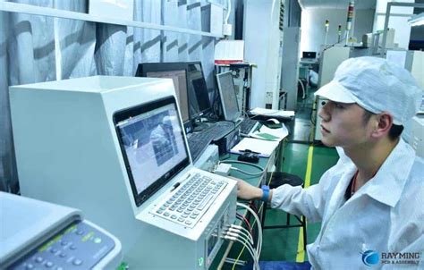
Visual Inspection
Visual inspection is the first step in PCB testing. It involves examining the PCB for any visible defects, such as:
- Incorrect component placement
- Solder bridges or shorts
- Damaged or missing components
- Incorrect labeling or marking
This process can be performed manually by trained operators or using automated optical inspection (AOI) systems.
Automated Optical Inspection (AOI)
AOI systems use high-resolution cameras and advanced image processing algorithms to detect defects on PCBs. The benefits of using AOI include:
- High-speed inspection
- Consistent and accurate results
- Ability to detect defects that may be missed by manual inspection
- Reduced labor costs
X-Ray Inspection
X-ray inspection is used to detect defects that are not visible on the surface of the PCB, such as:
- Voids in solder joints
- Insufficient solder coverage
- Misaligned or missing components
X-ray inspection systems use high-energy X-rays to create images of the internal structure of the PCB, allowing for the detection of hidden defects.
In-Circuit Testing (ICT)
In-circuit testing is a technique used to test the functionality of individual components on a PCB. It involves using a bed-of-nails fixture to make electrical contact with specific points on the PCB and measuring the electrical characteristics of the components. ICT can detect issues such as:
- Open or short circuits
- Incorrect component values
- Missing or damaged components
Flying Probe Testing
Flying probe testing is an alternative to ICT that uses movable probes to make electrical contact with specific points on the PCB. This technique offers several advantages over ICT, including:
- No need for a custom bed-of-nails fixture
- Ability to test a wide variety of PCB designs
- Faster setup times
Boundary Scan Testing
Boundary scan testing, also known as JTAG testing, is a technique used to test the interconnections between components on a PCB. It involves using a special test access port (TAP) to control and monitor the inputs and outputs of the components. Boundary scan testing can detect issues such as:
- Open or short circuits between components
- Incorrect Component Orientation
- Defective or damaged components

Types of PCBA Testing Techniques
Functional Testing
Functional testing is used to verify that a PCBA performs according to its intended specifications. This type of testing involves applying input signals to the PCBA and measuring the output signals to ensure they meet the expected values. Functional testing can be performed using various methods, such as:
- In-circuit emulation (ICE)
- Boundary scan testing
- Automated test equipment (ATE)
Burn-In Testing
Burn-in testing is used to identify PCBAs that are likely to fail early in their lifetime. It involves subjecting the PCBA to elevated temperatures and voltages for an extended period to accelerate the aging process. PCBAs that survive the burn-in process are more likely to have a longer lifespan in the field.
Environmental Testing
Environmental testing is used to evaluate the performance of a PCBA under various environmental conditions, such as:
- Temperature extremes
- Humidity
- Vibration
- Shock
This type of testing helps ensure that the PCBA can withstand the intended operating environment and maintain its functionality over time.
Electromagnetic Compatibility (EMC) Testing
EMC testing is used to ensure that a PCBA does not generate excessive electromagnetic interference (EMI) and is not susceptible to external EMI sources. This type of testing involves measuring the electromagnetic emissions from the PCBA and subjecting it to various EMI sources to evaluate its immunity.

Test Equipment and Tools
To perform PCB and PCBA testing, various equipment and tools are used, including:
- Multimeters
- Oscilloscopes
- Logic analyzers
- Signal generators
- Power supplies
- Thermal chambers
- Vibration and shock test systems
- EMC test chambers
| Equipment/Tool | Purpose |
|---|---|
| Multimeter | Measure voltage, current, and resistance |
| Oscilloscope | Analyze and display waveforms |
| Logic Analyzer | Capture and analyze digital signals |
| Signal Generator | Generate test signals for functional testing |
| Power Supply | Provide stable power for testing |
| Thermal Chamber | Simulate temperature extremes for environmental testing |
| Vibration System | Simulate vibration conditions for environmental testing |
| EMC Test Chamber | Evaluate electromagnetic compatibility |

Test Coverage and Metrics
To ensure the effectiveness of PCB and PCBA testing, it is important to establish test coverage and metrics. Test coverage refers to the percentage of the PCB or PCBA that is tested, while metrics are used to measure the effectiveness of the testing process.
Common test coverage and metrics include:
- Defect detection rate
- False failure rate
- First pass yield
- Defects per million opportunities (DPMO)
- Test coverage percentage
By monitoring these metrics, manufacturers can continuously improve their testing processes and ensure the highest quality products.
Best Practices for PCB and PCBA Testing
To optimize the effectiveness of PCB and PCBA testing, consider the following best practices:
- Develop a comprehensive test plan that covers all aspects of the PCB or PCBA
- Use a combination of testing techniques to ensure maximum coverage
- Establish clear acceptance criteria for each test
- Regularly calibrate and maintain test equipment
- Provide adequate training for test operators
- Continuously monitor and analyze test results to identify areas for improvement
Frequently Asked Questions (FAQ)
- What is the difference between PCB and PCBA testing?
-
PCB testing focuses on the bare printed circuit board, while PCBA testing involves testing the board with components already assembled.
-
Is visual inspection sufficient for PCB testing?
-
While visual inspection is an important first step, it should be combined with other testing techniques to ensure comprehensive coverage.
-
What are the benefits of using automated test equipment (ATE) for PCBA testing?
-
ATE offers high-speed, consistent, and accurate testing, reducing the need for manual labor and increasing test coverage.
-
How often should test equipment be calibrated?
-
Test equipment should be calibrated according to the manufacturer’s recommendations or industry standards, typically at least once a year.
-
What is the importance of environmental testing for PCBAs?
- Environmental testing ensures that the PCBA can withstand the intended operating conditions and maintain its functionality over time, reducing the risk of failures in the field.
Conclusion
PCB and PCBA testing are essential processes in the manufacturing of electronic devices. By employing a combination of testing techniques, such as visual inspection, AOI, X-ray inspection, ICT, flying probe testing, boundary scan testing, functional testing, burn-in testing, environmental testing, and EMC testing, manufacturers can ensure the highest quality and reliability of their products.
Establishing test coverage and metrics, following best practices, and continuously monitoring and improving the testing process are key to achieving success in PCB and PCBA testing.


Leave a Reply