Introduction
Printed circuit boards (PCBs) are essential components in nearly all modern electronics, from computers and smartphones to medical devices and vehicles. As electronic devices continue advancing in capabilities while shrinking in size, the PCBs inside them must evolve as well. This is where multech PCBs come into play.
Multech PCBs provide several advantages over traditional PCBs that make them ideal for today’s increasingly complex and compact electronics. In this article, we’ll explore what exactly multech PCBs are, their key benefits, and why they’ve become so ubiquitous in cutting-edge devices. We’ll also look at some of the top multech PCB manufacturers leading innovation in this field.
What Are Multech PCBs?

Multech PCBs are printed circuit boards constructed using multiple layers of circuitry stacked together, as opposed to single or double layer PCBs. The term “multech” itself is short for “multilayer technology”.
While early PCBs contained just a single conductive layer, advances in manufacturing techniques enabled the development of multilayer PCBs. This allowed more complex circuit designs by providing more space to route traces and components.
In multech PCBs, conductive layers are interleaved with insulating dielectric layers that provide separation and prevent short circuits. Vias are drilled holes filled with conductive material that provide electrical connections between layers.
Here is a comparison of single, double, and multilayer PCB configurations:
| PCB Type | Number of Conductive Layers | Number of Dielectric Layers |
|---|---|---|
| Single Layer | 1 | 0 |
| Double Layer | 2 | 1 |
| Multilayer | 4+ | 3+ |
Modern high-end multech PCBs can contain 8 or more layers, with some exceeding 30 layers for extremely complex, dense designs. The increased routing area and flexibility empower multech PCBs to house more components and circuitry in less space compared to earlier PCB technologies.
Benefits of Multech PCBs
Multech PCBs provide several key advantages that make them well-suited for modern, cutting-edge electronics:
Smaller Size
The mulitlayer design of multech PCBs allows more components and circuitry to fit onto a smaller board area. This enables smaller and more portable devices. Multech PCBs were instrumental in enabling the progression from bulky desktops to slim laptops and mobile devices.
Increased Performance
With more layers, multech PCBs can accommodate higher density component mounting and faster circuit traces. This leads to improved functionality, speed, and computing power compared to single or double layer PCBs.
Lower Noise
Separating analog and digital signals onto different layers reduces electromagnetic interference noise. This results in clearer audio, video, and data signals.
Better Heat Dissipation
The multiple layers allow wider, thicker copper planes that spread heat more efficiently. This improves thermal management and component lifespan.
Higher Reliability
Vias and redundant circuits paths in multech PCBs offer backup connectivity if a trace is damaged, enhancing reliability. The multilayer structure is also inherently more resistant to vibrations and shocks.
Design Flexibility
With more routing layers, multech PCB layouts can accommodate last-minute circuit changes more easily compared to fewer-layer boards.
In summary, multech PCBs enable smaller, better performing, and more reliable electronics. Their advantages have established them as the PCB technology of choice for nearly all modern compact devices and high-speed circuits.
Multech PCB Manufacturing
Producing multech PCBs requires advanced manufacturing capabilities beyond that of single or double layer boards. Several key steps are involved:
Layer Stackup
The layer stackup refers to the sequence of conductive copper and insulating dielectric layers that make up the multech board. The layer stackup is carefully engineered to optimize electrical performance and meet circuit density requirements.
Registration
Accurately aligning (registering) the layers is critical so vias correctly interconnect the traces between layers. High-precision laser drilling forms the interlayer vias.
Lamination
The conductive and dielectric layers are pressed and bonded together into a solid board under heat and pressure.
Trace Imaging
Photolithographic processes transfer the circuit patterns onto the copper layers.
Plating and Coating
Plating deposits conductors in vias and through-holes. Special coatings like solder masks, silkscreens, and finishes are applied.
Testing
Rigorous electrical testing checks for layer alignment, continuity, and function.
Multech PCB fabrication requires substantial investment in advanced equipment, engineering expertise, and quality control. Leading multech PCB manufacturers are at the forefront of high-density PCB technology.
Major Multech PCB Manufacturers

Many companies manufacture multech PCBs, but a few giants dominate the high-volume, high-complexity PCB fabrication market:
TTM Technologies
One of the top global PCB manufacturers, TTM specializes in complex, high-density multech boards for cellphones, medical products, aerospace, and automotive applications.
AT&S
An Austrian-based company focused on mobile and automotive multech PCBs using the latest techniques like embedded die packaging and in-mold electronics.
Zhen Ding Tech
The largest PCB supplier in Taiwan and a leading multech board maker for consumer electronics and communications products.
Tripod Technology
Another major Taiwanese PCB company focused on multech boards for notebook PCs, servers, and networking equipment.
Unimicron Technology
Known for high-quality rigid and flexible multech PCBs meeting tight tolerances for telecom infrastructure and mobile devices.
Nan Ya PCB
A Taiwan multech PCB maker supplying products extensively used in laptops, smartphones, TVs, and networking gear.
The Future of Multech PCBs
As electronics developers pack more performance and functions into ever-smaller packages, demand for leading-edge multech PCB technology continues growing. Here are some emerging trends:
Finer Features
Manufacturing enhancements will enable shrinking feature sizes below 5 microns to increase circuit densities. This allows packing more capabilities into small products.
Embedded Components
More components like capacitors and resistors will be embedded into the multech PCB itself rather than mounted on the surface. This further reduces size and enhances reliability.
HDI Technology
High-density interconnect (HDI) multech PCBs with microvias, tight tolerances, and stacked vias will accommodate greater component densities and thinner end products.
Flex-Rigid Designs
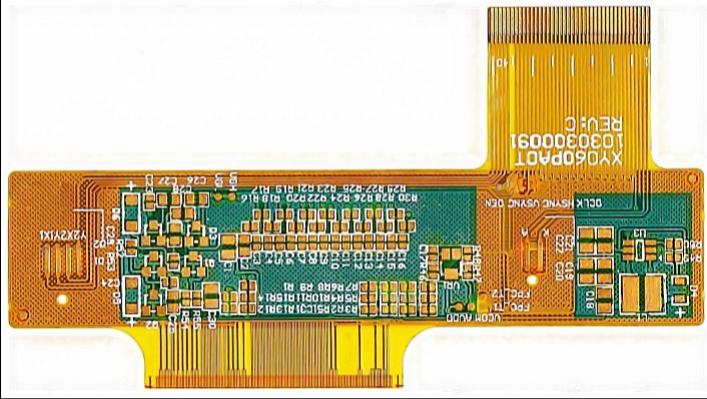
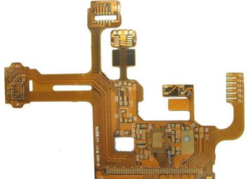
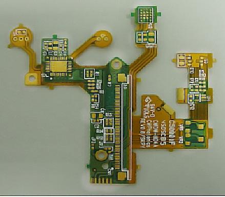
Combining rigid and flexible substrates in one multech PCB will allow more efficient and space-saving circuit layouts.
Metal Core PCBs
Multech PCBs with a thermally conductive metal core provide enhanced cooling for high-power circuits and allow thinner form factors.
Additive Manufacturing
Emerging 3D printing of PCB conductors will enable more complex multech designs not possible with traditional etching.
Conclusion
Multech PCBs have progressed leaps and bounds from the earliest single-layer circuit boards developed decades ago. The advanced mulitlayer PCB designs being produced today provide the circuit densities, performance, and reliability needed to power cutting-edge electronics like smartphones, tablets, IoT devices, high-speed telecom infrastructure, and vehicle electronics. Continued multech PCB technology advances will help drive innovation in these fields in the future. Leading PCB manufacturers investing in next-generation multech fabrication methods will be positioned to support the needs of electronics companies worldwide.
Frequently Asked Questions
What are the key benefits of multech PCBs?
The main benefits of multech PCBs are smaller size, increased performance and speed, lower noise, better heat dissipation, higher reliability, and greater design flexibility compared to single or double layer PCBs.
How many layers do modern high-end multech PCBs have?
Advanced multech PCBs today often have 8 to 16 layers, but some exceed 30 layers for extremely complex, dense circuit designs required in products like smartphones.
What are some emerging trends in multech PCB technology?
Key trends include shrinking feature sizes, embedded passives, high-density interconnects, flex-rigid designs, metal core PCBs, and additive manufacturing. These will enable greater circuit densites and capabilities.
What are some leading multech PCB manufacturers?
Major global multech PCB makers include TTM Technologies, AT&S, Zhen Ding Tech, Tripod Technology, Unimicron Technology, and Nan Ya PCB.
Why have multech PCBs become so ubiquitous?
The small size, improved performance, noise reduction, thermal dissipation, reliability, and design flexibility of multech PCBs have made them ideal for today’s increasingly sophisticated, compact consumer and commercial electronics.


Leave a Reply