Introduction to PCB Components in Mobile Phones
Printed Circuit Boards (PCBs) are the backbone of modern electronics, including mobile cell phones. These complex boards house various components that work together to enable the functionality of a cell phone. Understanding the different parts and components on a mobile phone’s PCB can be helpful for technicians, engineers, and curious individuals who want to learn more about the inner workings of these devices.
In this article, we will explore the key components found on a typical mobile phone PCB and provide guidance on how to identify them.
Main Components on a Mobile Phone PCB
1. Processor (CPU)
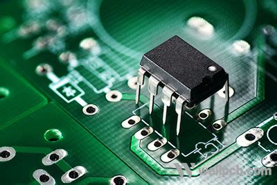
The processor, also known as the Central Processing Unit (CPU), is the “brain” of the mobile phone. It handles all the computational tasks and controls the overall functionality of the device. The processor is usually the largest chip on the PCB and is often located near the center of the board.
To identify the processor, look for a large, square-shaped chip with multiple pins on all sides. The processor will typically have the manufacturer’s name and model number printed on it.
2. Memory (RAM and ROM)
Mobile phones utilize two types of memory: Random Access Memory (RAM) and Read-Only Memory (ROM). RAM is used for temporary storage of data and instructions while the phone is in use, while ROM holds the phone’s operating system and other permanent software.
Memory chips are usually smaller than the processor and are located near it on the PCB. They are often rectangular in shape and have multiple pins on two sides. The type of memory (RAM or ROM) and its capacity may be printed on the chip.
3. Storage (Flash Memory)
Flash memory is used for long-term storage of data, such as photos, videos, and apps. In most modern smartphones, the flash memory is integrated into the device and is not easily accessible on the PCB.
However, in some older or lower-end phones, the flash memory may be a separate chip on the PCB. It will typically be a rectangular chip with multiple pins and may have the capacity printed on it (e.g., 8GB, 16GB, etc.).
4. Power Management IC (PMIC)
The Power Management Integrated Circuit (PMIC) is responsible for managing the Power Supply to the various components on the PCB. It ensures that each component receives the correct voltage and current, and it also helps to optimize battery life.
The PMIC is usually a small, rectangular chip located near the battery connector. It may have multiple pins on two or four sides and will often have the manufacturer’s name and model number printed on it.
5. Radio Frequency (RF) Components
RF components are responsible for the mobile phone’s wireless communication capabilities, such as cellular network connectivity, Wi-Fi, Bluetooth, and GPS. These components include:
- Baseband processor: Handles the digital signal processing for wireless communication.
- RF transceiver: Transmits and receives radio signals.
- Power amplifier: Amplifies the radio signals for transmission.
- Antenna switch: Switches between different antennas for various frequencies and Communication Protocols.
RF components are usually located together on one end of the PCB, near the antenna connectors. They may be shielded by metal covers to reduce electromagnetic interference.
6. Audio Components
Audio components enable the mobile phone’s sound input and output capabilities, such as the microphone, speaker, and headphone jack. These components include:
- Audio codec: Converts digital audio signals to analog and vice versa.
- Audio amplifier: Amplifies the analog audio signals for the speaker or headphone output.
Audio components are typically located near the edge of the PCB, close to the microphone and speaker connectors.
7. Display and Touch Interface
The display and touch interface components handle the visual output and touch input of the mobile phone. These components may include:
- Display connector: Connects the PCB to the phone’s display module.
- Touch controller: Processes touch input from the phone’s touchscreen.
These components are usually located along the edge of the PCB, near the display connector.
8. Sensors
Modern smartphones incorporate various sensors to enable features like screen orientation, motion detection, and environmental sensing. Common sensors found on a mobile phone PCB include:
- Accelerometer: Detects the phone’s orientation and motion.
- Gyroscope: Measures the phone’s angular velocity and rotation.
- Proximity Sensor: Detects the presence of nearby objects, such as when the phone is held close to the user’s face during a call.
- Ambient light sensor: Measures the surrounding light levels to adjust the display brightness automatically.
Sensors are typically small, rectangular chips located at various points on the PCB, depending on their function and the phone’s design.

Visual Guide to Mobile Phone PCB Components
| Component | Appearance | Location |
|---|---|---|
| Processor (CPU) | Large, square chip with multiple pins | Near the center of the PCB |
| Memory (RAM and ROM) | Smaller, rectangular chips with pins on two sides | Near the processor |
| Storage (Flash Memory) | Rectangular chip with pins, capacity printed on it | Integrated into the device, not easily accessible |
| Power Management IC (PMIC) | Small, rectangular chip near the battery connector | Near the battery connector |
| RF Components | Shielded by metal covers, located together | One end of the PCB, near antenna connectors |
| Audio Components | Small chips near microphone and speaker connectors | Near the edge of the PCB |
| Display and Touch Interface | Components located along the edge, near display connector | Edge of the PCB |
| Sensors | Small, rectangular chips at various locations | Various points on the PCB, depending on function |

Tips for Identifying PCB Components
- Use a magnifying glass or microscope to examine the PCB closely, as some components may be very small.
- Look for printed labels or markings on the components, which often indicate their function or specification.
- Consult the phone’s service manual or schematic diagram, if available, to help identify specific components and their locations on the PCB.
- Compare the PCB to images or diagrams of similar phone models to identify components by their appearance and location.
- Utilize online resources, such as electronics forums or repair guides, for additional information and guidance on identifying PCB components.

Frequently Asked Questions (FAQ)
1. Can I replace a faulty component on my mobile phone’s PCB myself?
While it is possible to replace some components on a mobile phone PCB, it is generally not recommended for individuals without proper training and equipment. Attempting to replace components yourself may cause further damage to the device and void any warranties. It is best to seek the assistance of a professional repair service.
2. How can I tell if a component on my phone’s PCB is damaged?
Identifying a damaged component on a PCB can be challenging without proper diagnostic tools and knowledge. Some signs of a damaged component may include:
- Visible damage, such as burn marks, cracks, or deformities
- Unusual behavior of the phone, such as overheating, unexpected shutdowns, or specific features not working properly
If you suspect a component is damaged, it is best to have the device examined by a professional repair service.
3. Are the PCB components the same in all mobile phones?
While the basic types of components found on mobile phone PCBs are similar across different models and brands, the specific components used may vary. Factors such as the phone’s features, performance requirements, and design can influence the choice of components. Additionally, component manufacturers may update or discontinue certain parts over time, leading to variations in the components used in different phone models.
4. Can I upgrade the components on my mobile phone’s PCB to improve performance?
In most cases, upgrading individual components on a mobile phone’s PCB is not possible or practical. Mobile phone PCBs are designed with specific components in mind, and changing them can lead to compatibility issues or even damage to the device. The best way to improve a phone’s performance is to purchase a newer model with updated hardware and features.
5. How do I safely clean my mobile phone’s PCB?
If you need to clean your mobile phone’s PCB, it is essential to take proper precautions to avoid damaging the components. Here are some steps to safely clean a PCB:
- Power off the device and remove the battery, if possible.
- Use compressed air to blow away any loose dust or debris gently.
- If necessary, use a soft-bristled brush to carefully remove any remaining dirt or grime.
- For more stubborn dirt, use a small amount of isopropyl alcohol on a lint-free cloth or swab to gently clean the affected areas. Be sure to avoid getting alcohol on any exposed connectors or components.
- Allow the PCB to dry completely before reassembling the device and powering it on.
Remember, if you are unsure about cleaning your phone’s PCB or encounter any difficulties, it is best to seek the assistance of a professional repair service.
Conclusion
Understanding the various parts and components on a mobile phone’s PCB can be valuable for technicians, engineers, and anyone interested in the inner workings of these devices. By familiarizing yourself with the appearance and location of key components, such as the processor, memory, RF components, and sensors, you can better diagnose issues and appreciate the complexity of modern mobile phones.
However, it is essential to remember that working with mobile phone PCBs requires proper training, tools, and expertise. Always take necessary precautions and seek professional assistance when attempting repairs or modifications to ensure the best possible outcome for your device.


Leave a Reply