Introduction
In the ever-evolving world of electronics, the demand for efficient and reliable wireless communication systems has skyrocketed. From smartphones and Wi-Fi routers to radar systems and satellite communications, radio frequency (RF) technology plays a crucial role in enabling these applications. At the heart of RF systems lies a specialized type of printed circuit board (PCB) designed to handle the unique challenges of high-frequency signals: the RF PCB.
RF PCBs are essential components in a wide range of electronic devices that transmit, receive, or process radio frequency signals. These specialized PCBs are engineered to meet stringent requirements, such as low signal loss, controlled impedance, and minimal electromagnetic interference (EMI). Understanding the intricacies of RF PCB design is vital for ensuring the reliable and efficient operation of RF systems.
In this comprehensive article, we will explore the world of RF PCBs, delving into their unique characteristics, design considerations, materials, and manufacturing processes. We will also discuss the various applications of RF PCBs and the challenges associated with their design and implementation. Whether you are an electronics engineer, a hobbyist, or simply curious about this fascinating technology, this article will provide you with a solid foundation in understanding RF PCBs.
What is a RF PCB?
A radio frequency (RF) PCB is a specialized type of printed circuit board specifically designed to handle high-frequency signals in the radio frequency spectrum. Unlike conventional PCBs used for digital and low-frequency analog circuits, RF PCBs are engineered to address the unique challenges posed by high-frequency signals, such as signal integrity, impedance control, and electromagnetic compatibility (EMC).
RF PCBs are essential components in a wide range of wireless communication systems, including:
- Cellular networks (2G, 3G, 4G, 5G)
- Wi-Fi and Bluetooth devices
- Radar systems
- Satellite communications
- Radio broadcasting
- Wireless sensor networks
- RFID (Radio Frequency Identification) systems
These specialized PCBs are designed to transmit, receive, and process radio frequency signals efficiently, while minimizing signal loss, distortion, and interference.
Key Characteristics of RF PCBs
RF PCBs possess several unique characteristics that set them apart from conventional PCBs. These characteristics are crucial for ensuring the reliable and efficient operation of RF systems:
1. Controlled Impedance
In RF circuits, it is essential to maintain a consistent and well-defined impedance to minimize signal reflections and ensure proper signal propagation. RF PCBs are designed with controlled impedance traces, which means that the trace width, thickness, and dielectric properties are carefully calculated to achieve the desired characteristic impedance, typically 50 ohms.
2. Low Signal Loss
At high frequencies, signal loss can become a significant issue due to factors such as conductor and dielectric losses. RF PCBs are engineered to minimize signal loss by using low-loss materials and optimizing trace geometries, ensuring that signals are transmitted and received with minimal attenuation.
3. Electromagnetic Compatibility (EMC)
RF circuits can be susceptible to electromagnetic interference (EMI) from external sources or internal cross-talk between traces. RF PCBs are designed with EMC in mind, incorporating features such as ground planes, shielding layers, and careful trace routing to minimize EMI and ensure reliable signal transmission.
4. High-Frequency Materials
RF PCBs often utilize specialized materials that are optimized for high-frequency applications. These materials exhibit desirable properties such as low dielectric loss, good thermal conductivity, and dimensional stability, ensuring reliable performance at high frequencies.
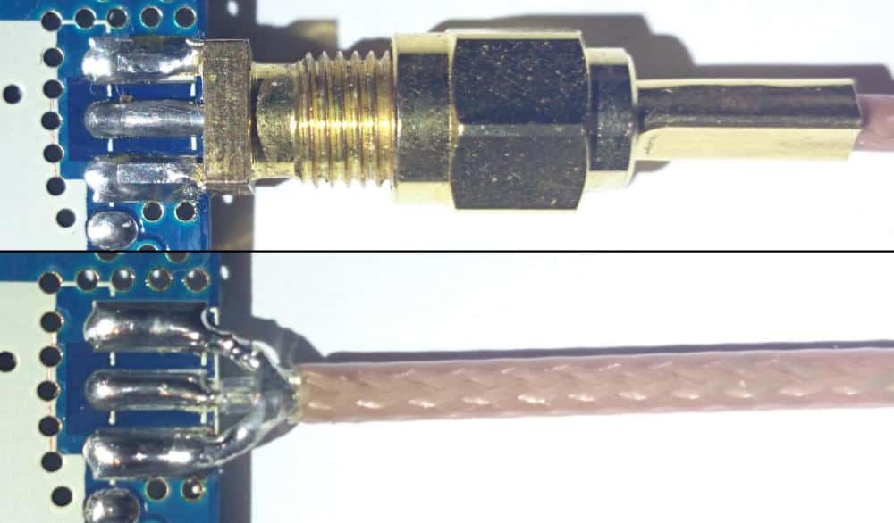
5. Grounding and Shielding
Proper grounding and shielding are essential in RF PCB design to minimize signal interference and ensure electromagnetic compatibility. RF PCBs typically incorporate features such as ground planes, shielding layers, and careful layout techniques to achieve effective grounding and shielding.
6. Thermal Management
RF circuits can generate significant amounts of heat, particularly in high-power applications. RF PCBs are designed with thermal management considerations, such as the use of specialized materials with good thermal conductivity and the incorporation of heat sinks or specialized cooling solutions.
RF PCB Design Considerations
Designing an RF PCB requires a deep understanding of high-frequency signal behavior and the unique challenges associated with RF systems. Here are some key design considerations for RF PCBs:
1. Signal Integrity
Signal integrity is of utmost importance in RF PCB design. This involves ensuring that the signal remains undistorted and free from interference as it propagates through the PCB. Factors such as trace geometries, impedance control, and careful layout techniques play a crucial role in maintaining signal integrity.
2. Impedance Matching
Impedance mismatches can lead to signal reflections and power losses in RF circuits. RF PCB designers must carefully match the impedance of the traces, components, and interconnections to minimize these issues and ensure efficient signal transmission.
3. Crosstalk and Electromagnetic Interference (EMI)
In RF PCBs, crosstalk and EMI can significantly degrade signal quality and system performance. Careful trace routing, shielding, and grounding techniques are employed to minimize these effects and ensure reliable operation.
4. Power Integrity
RF circuits often involve high-power signals, which can lead to issues such as voltage drops, ground bounces, and electromagnetic radiation. RF PCB designers must consider power integrity by incorporating appropriate decoupling capacitors, power plane designs, and efficient power distribution networks.
5. Thermal Management
High-frequency signals and high-power RF components can generate significant amounts of heat, which can adversely affect performance and reliability. RF PCB designers must account for thermal management by incorporating heat sinks, thermal vias, or other cooling solutions to dissipate heat effectively.
6. Manufacturing Considerations
RF PCBs often require specialized manufacturing processes and techniques to achieve the desired performance. Factors such as material selection, layer stackup, and fabrication tolerances must be carefully considered to ensure consistent and reliable production.
RF PCB Materials
The choice of materials plays a crucial role in the performance and reliability of RF PCBs. Here are some common materials used in RF PCB manufacturing:
1. Substrates
RF PCBs often utilize specialized substrates optimized for high-frequency applications. Common substrate materials include:
- FR-4: A cost-effective and widely used material, suitable for lower frequency applications.
- Rogers RT/duroid: A high-performance material with low dielectric loss and good dimensional stability, suitable for high-frequency applications.
- PTFE (Polytetrafluoroethylene): A low-loss material with excellent electrical properties, commonly used in high-frequency and high-power RF applications.
- Ceramic-filled composites: Materials with ceramic fillers, offering low dielectric loss and high thermal conductivity, suitable for high-power and high-frequency applications.
2. Conductive Materials
The conductive materials used in RF PCBs play a crucial role in signal transmission and power distribution:
- Copper: The most commonly used conductive material in PCBs due to its excellent electrical conductivity and availability.
- Aluminum: An alternative conductive material with lower cost and weight, but higher resistivity compared to copper.
- Conductive polymers: Specialized conductive polymers can be used for applications requiring flexibility or shielding properties.
3. Solder Masks and Conformal Coatings
Solder masks and conformal coatings are applied to RF PCBs to protect the conductive traces and components from environmental factors such as moisture, chemicals, and physical damage. These materials must be carefully chosen to ensure compatibility with the operating frequencies and avoid introducing signal degradation or interference.
RF PCB Manufacturing Processes
The manufacturing process for RF PCBs requires specialized techniques and equipment to achieve the desired performance and reliability. Here are some common manufacturing processes used for RF PCBs:
1. Material Selection and Layer Stackup
The selection of appropriate substrate materials and the design of the layer stackup are critical steps in RF PCB manufacturing. The layer stackup determines the distribution of signal layers, ground planes, and power planes, which directly impacts signal integrity, impedance control, and EMI performance.
2. Trace Formation
RF PCBs often require precise trace formation techniques to achieve the desired trace geometries and impedance control. Common methods include etching, laser direct imaging, and semi-additive processes, which offer tight tolerances and high-resolution patterning.
3. Plating and Surface Finishing
Plating and surface finishing processes are essential for RF PCBs to ensure reliable electrical connections and prevent oxidation or corrosion. Common plating materials include gold, silver, and tin-lead alloys, while surface finishes like immersion silver, electroless nickel/immersion gold (ENIG), and hot air solder leveling (HASL) are widely used.
4. Lamination and Multilayer Construction
Many RF PCBs require multiple layers to accommodate complex circuit designs and interconnections. The lamination process involves bonding multiple layers of copper-clad dielectric materials under high temperature and pressure, creating a multilayer PCB structure.
5. Drilling and Via Formation
Precise drilling and via formation are crucial for RF PCBs to ensure reliable interconnections between layers and minimize signal degradation. Advanced techniques like laser drilling, mechanical drilling, and blind/buried vias may be employed depending on the design requirements.
6. Testing and Quality Control
Rigorous testing and quality control procedures are essential for RF PCBs to ensure compliance with design specifications and performance requirements. Electrical testing, impedance measurements, and signal integrity analyses are commonly performed to validate the PCB’s functionality and identify potential issues.
Applications of RF PCBs
RF PCBs are essential components in a wide range of applications that rely on wireless communication and high-frequency signal processing. Here are some key applications of RF PCBs:
1. Telecommunications
RF PCBs are at the heart of telecommunication systems, including cellular networks (2G, 3G, 4G, 5G), satellite communications, and radio broadcasting. These PCBs facilitate the transmission and reception of high-frequency signals, enabling reliable and efficient wireless communication.
2. Wireless Networking
Wi-Fi routers, access points, and various wireless networking devices rely on RF PCBs to transmit and receive data over radio frequencies. These PCBs are designed to handle multiple frequency bands and ensure reliable connectivity in wireless local area networks (WLANs).
3. Radar Systems
RF PCBs play a crucial role in radar systems used for air traffic control, weather monitoring, and military applications. These PCBs are designed to handle high-frequency signals, enabling precise detection and tracking of targets through the transmission and reception of radio waves.
4. Wireless Sensors and IoT Devices
The Internet of Things (IoT) and wireless sensor networks rely heavily on RF PCBs for data transmission and communication between devices. These PCBs enable low-power, long-range communication in applications such as environmental monitoring, industrial automation, and smart home systems.
5. RFID (Radio Frequency Identification)
RFID systems use RF PCBs to transmit and receive radio frequency signals for the purpose of identifying and tracking objects. These PCBs are found in various RFID applications, including supply chain management, access control, and asset tracking.
6. Automotive and Aerospace Electronics
RF PCBs are employed in automotive and aerospace electronics for applications such as vehicle-to-vehicle communication, collision avoidance systems, and in-flight entertainment systems. These PCBs must be designed to withstand harsh environmental conditions and meet stringent reliability standards.
Challenges and Future Trends in RF PCB Design
Despite the advancements in RF PCB technology, several challenges and future trends continue to shape the development of these specialized PCBs:
1. Miniaturization and Integration
As electronic devices become increasingly compact, there is a growing demand for miniaturized and highly integrated RF PCBs. This poses challenges in terms of component packaging, thermal management, and signal integrity, requiring innovative design solutions and manufacturing techniques.
2. Higher Frequencies and Wider Bandwidths
The ever-increasing demand for higher data rates and faster wireless communication is driving the need for RF PCBs capable of operating at higher frequencies and supporting wider bandwidths. This necessitates the development of new materials, design techniques, and manufacturing processes to ensure reliable performance at these higher frequencies.
3. Electromagnetic Compatibility (EMC) Challenges
As the number of wireless devices and systems continues to grow, the risk of electromagnetic interference (EMI) and compatibility issues increases. RF PCB designers must continuously improve shielding, grounding, and layout techniques to mitigate EMI and ensure reliable operation in crowded electromagnetic environments.
4. Thermal Management Advancements
High-power RF applications, such as radar systems and wireless base stations, require advanced thermal management solutions to dissipate heat effectively and maintain reliable operation. This may involve the development of new materials with improved thermal conductivity, as well as innovative cooling techniques and heat sink designs.
5. Additive Manufacturing and 3D Printing
Additive manufacturing and 3D printing technologies are expected to have a significant impact on the production of RF PCBs in the future. These techniques offer the potential for customized and complex geometries, as well as the integration of multiple materials and components within a single PCB structure.
6. Artificial Intelligence (AI) and Machine Learning (ML) in Design
The complexity of RF PCB design and the increasing demand for optimized performance are driving the adoption of artificial intelligence (AI) and machine learning (ML) techniques. These technologies can assist in automating design processes, optimizing layouts, and predicting performance characteristics, potentially leading to more efficient and reliable RF PCB designs.
Frequently Asked Questions (FAQ)
- What makes RF PCBs different from conventional PCBs? RF PCBs are specifically designed to handle high-frequency signals in the radio frequency spectrum. They incorporate features such as controlled impedance, low signal loss, and electromagnetic compatibility (EMC) to ensure reliable and efficient operation at these higher frequencies.
- Why is controlled impedance important in RF PCB design? Controlled impedance is crucial for minimizing signal reflections and ensuring proper signal propagation in RF circuits. RF PCBs are designed with carefully calculated trace geometries and dielectric properties to achieve the desired characteristic impedance, typically 50 ohms.
- What materials are commonly used in RF PCB manufacturing? Common materials used in RF PCB manufacturing include specialized substrates like Rogers RT/duroid, PTFE, and ceramic-filled composites, as well as conductive materials like copper and aluminum. The choice of materials depends on factors such as frequency range, power requirements, and performance specifications.
- How does the manufacturing process for RF PCBs differ from conventional PCBs? RF PCB manufacturing often requires specialized techniques and equipment to achieve the desired performance and reliability. This includes precise trace formation methods, advanced plating and surface finishing processes, and rigorous testing and quality control procedures.
- What are some common applications of RF PCBs? RF PCBs are widely used in applications such as telecommunications (cellular networks, satellite communications), wireless networking (Wi-Fi, Bluetooth), radar systems, wireless sensors and IoT devices, RFID systems, and automotive and aerospace electronics.
Conclusion
RF PCBs are specialized printed circuit boards designed to handle the unique challenges of high-frequency signal transmission and processing. With their controlled impedance, low signal loss, and electromagnetic compatibility features, RF PCBs are essential components in a wide range of wireless communication systems and applications.
As the demand for faster and more reliable wireless technologies continues to grow, the importance of RF PCB design and manufacturing will only increase. Advancements in materials, manufacturing processes, and design techniques will be crucial to address challenges such as miniaturization, higher frequencies, thermal management, and electromagnetic compatibility.
Whether you are an engineer, a hobbyist, or simply interested in the fascinating world of wireless technology, understanding RF PCBs is a valuable asset. By mastering the principles and design considerations of these specialized PCBs, you can contribute to the development of cutting-edge wireless systems and drive innovation in a rapidly evolving technological landscape.


Leave a Reply