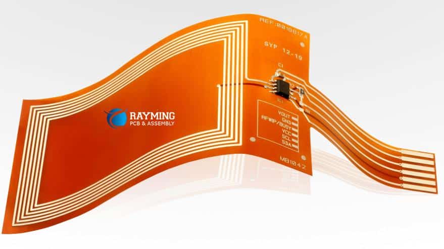
Designing a Radio Frequency (RF) Printed Circuit Board (PCB) requires specialized knowledge and techniques to ensure proper performance and signal integrity at high frequencies. RF PCBs are used in various applications, including wireless communication systems, radars, and RF instrumentation. This article will guide you through the key considerations and steps involved in designing an effective RF PCB.
Understanding RF Signal Characteristics
Before delving into the design process, it’s essential to understand the fundamental characteristics of RF signals and how they differ from lower-frequency signals:
- Wavelength: RF signals have shorter wavelengths compared to lower-frequency signals. This means that the physical dimensions of the PCB traces and components become more significant at higher frequencies, affecting signal propagation and impedance matching.
- Skin Effect: At higher frequencies, current tends to flow along the surface of conductors due to the skin effect. This phenomenon can increase resistance and affect signal integrity.
- Dielectric Losses: The dielectric materials used in PCBs can exhibit higher losses at RF frequencies, leading to signal attenuation and power dissipation.
- Electromagnetic Interference (EMI): RF signals are more susceptible to EMI from external sources and can also radiate unwanted emissions, requiring proper shielding and grounding techniques.
RF PCB Design Considerations
To ensure optimal RF performance, several design considerations must be addressed:
1. Controlled Impedance
Controlled impedance is crucial for maintaining signal integrity and minimizing reflections in RF PCBs. The target impedance is typically 50 ohms for most RF applications. Achieving controlled impedance involves carefully selecting the trace width, dielectric thickness, and dielectric constant of the PCB materials.
2. Trace Routing
Trace routing is critical in RF PCBs. Traces should be as short and straight as possible to minimize inductance and capacitance. Avoid sharp bends and right-angle turns, as they can introduce signal reflections and discontinuities.
3. Ground Planes
Proper grounding is essential for RF PCBs. Solid ground planes and low-impedance ground paths help reduce EMI, provide shielding, and improve signal return paths. Ensure that ground planes cover as much area as possible and are properly stitched together using multiple vias.
4. Decoupling and Bypass Capacitors
Decoupling and bypass capacitors are crucial for reducing noise and maintaining a stable power supply for RF circuits. Strategic placement of these capacitors near power pins and high-frequency components is essential.
5. Component Placement
Careful component placement is necessary to minimize parasitic effects and crosstalk. Place high-frequency components and sensitive circuits away from noise sources, such as digital circuits or high-current traces.
6. Thermal Management
RF circuits can generate significant heat, especially in high-power applications. Proper thermal management is essential to ensure reliable operation and prevent component degradation or failure.
RF PCB Design Process
Follow these steps to design an effective RF PCB:
1. Schematic Capture
Begin by creating a schematic diagram of the RF circuit, including all components, power supplies, and interconnections. Ensure that the schematic accurately represents the intended functionality and performance requirements.
2. Component Selection
Carefully select RF-specific components, such as low-noise amplifiers, mixers, filters, and oscillators, based on the desired frequency range, power levels, and performance requirements. Pay attention to component packages and footprints, as they can impact RF performance.
3. PCB Layout
Use a PCB layout tool specifically designed for RF applications. These tools often include features for controlled impedance routing, trace tuning, and electromagnetic simulation.
a. Stackup Design
Design the PCB stackup carefully, considering the dielectric material properties, layer thicknesses, and the number of signal and ground layers required for your RF design.
b. Trace Routing
Route the RF traces following best practices for controlled impedance and minimizing discontinuities. Use microstrip or stripline configurations as appropriate, and avoid crossing traces or high-density routing areas.
c. Ground and Power Planes
Create solid ground and power planes, ensuring proper stitching and low-impedance paths using multiple vias.
d. Component Placement
Place components strategically, considering signal flow, electromagnetic compatibility, and thermal management requirements.
e. Decoupling and Bypass Capacitors
Strategically place decoupling and bypass capacitors near power pins and high-frequency components to minimize noise and stabilize the power supply.
f. Thermal Management
Incorporate thermal management solutions, such as thermal vias, heat sinks, or specialized materials, depending on the power dissipation requirements of your RF design.
4. Simulation and Verification
Use electromagnetic simulation tools to analyze and verify the RF performance of your PCB design. These tools can simulate signal integrity, crosstalk, and electromagnetic compatibility (EMC) issues, allowing you to identify and address potential problems before manufacturing.
5. Design Rule Checking (DRC)
Perform a comprehensive Design Rule Checking (DRC) to ensure that your PCB design adheres to all manufacturing rules and constraints, such as minimum trace width, clearance, and via dimensions.
6. PCB Fabrication and Assembly
Once your RF PCB design is finalized and verified, prepare the necessary manufacturing files (e.g., Gerber files, drill files) and send them to a reputable PCB fabricator and assembly house specializing in RF products.
7. Testing and Verification
After assembly, thoroughly test and verify the performance of your RF PCB using appropriate test equipment, such as vector network analyzers, spectrum analyzers, and signal generators. Perform measurements and characterize the RF performance, including gain, noise figure, and frequency response.
FAQs
- What is the importance of controlled impedance in RF PCB design? Controlled impedance is crucial for maintaining signal integrity and minimizing reflections in RF PCBs. Uncontrolled impedance can lead to signal distortion, power loss, and overall degradation of RF performance.
- Why are ground planes essential in RF PCB design? Ground planes provide shielding, reduce EMI, and improve signal return paths in RF PCBs. They also help distribute heat and maintain a stable reference plane for controlled impedance routing.
- How do decoupling and bypass capacitors improve RF performance? Decoupling and bypass capacitors help reduce noise and maintain a stable power supply for RF circuits. They provide low-impedance paths for high-frequency noise and transients, preventing them from propagating through the circuit and degrading performance.
- What are the advantages of using specialized RF PCB design tools? RF PCB design tools offer features specifically tailored for high-frequency design, such as controlled impedance routing, trace tuning, and electromagnetic simulation. These tools can help ensure better signal integrity, minimize parasitic effects, and improve overall RF performance.
- Why is thermal management important in RF PCB design? RF circuits, especially in high-power applications, can generate significant heat. Proper thermal management is essential to ensure reliable operation and prevent component degradation or failure due to excessive temperatures.


Leave a Reply