Introduction
In the ever-evolving world of electronics, the quest for efficient and cost-effective manufacturing techniques has led to the exploration of 3D printing as a viable option for producing printed circuit boards (PCBs). While traditional methods of PCB fabrication have been well-established and widely used, the advent of additive manufacturing technologies, such as 3D printing, has opened up new possibilities for prototyping and small-scale production.
This article delves into the intriguing question of whether PCBs can be 3D printed, examining the current state of the technology, its advantages and limitations, and the potential impact it may have on the electronics industry. We will explore the various 3D printing techniques, materials, and processes that are being employed or investigated for PCB fabrication, as well as the challenges and considerations that must be addressed to make this approach more mainstream.
Conventional PCB Manufacturing Techniques
Before delving into the realm of 3D printed PCBs, it is essential to understand the traditional methods of PCB fabrication. These methods have been refined over decades and are widely used in the electronics industry due to their reliability, scalability, and cost-effectiveness for mass production.
Subtractive Manufacturing
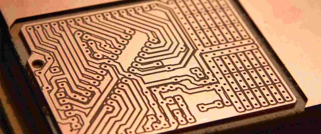
The most common technique for PCB manufacturing is subtractive manufacturing, also known as the “etch and plate” process. This method involves the following steps:
- A copper-clad laminate substrate is prepared.
- A photosensitive resist is applied to the copper surface.
- A pattern or design is transferred onto the resist using a photomask and UV light exposure.
- The exposed areas of the resist are removed, revealing the underlying copper.
- The exposed copper is then etched away, leaving the desired circuit pattern.
- Additional processes, such as electroplating or surface finishing, may be applied to enhance the PCB’s characteristics.
This subtractive method effectively removes unwanted copper from the substrate, leaving behind the desired circuit traces and component pads.
Additive Manufacturing
An alternative to subtractive manufacturing is additive manufacturing, where conductive materials are selectively deposited onto a substrate to create the desired circuit pattern. Examples of additive manufacturing techniques for PCBs include:
- Inkjet Printing: This method uses conductive inks, typically containing metal nanoparticles, which are precisely deposited onto a substrate using inkjet printing technology.
- Aerosol Jet Printing: Similar to inkjet printing, but using an aerosol stream of conductive material instead of liquid ink.
- Laser Direct Structuring (LDS): A laser beam activates specific areas of a plastic substrate, enabling the selective deposition of conductive materials onto those activated areas.
While additive manufacturing techniques offer advantages such as reduced material waste and the ability to create complex geometries, they are typically used for prototyping or low-volume production due to limitations in resolution, conductivity, and scalability.
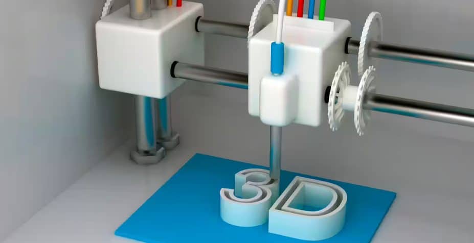
3D Printing for PCB Fabrication
The application of 3D printing technology to PCB fabrication has garnered significant interest in recent years, driven by the potential benefits it offers, such as rapid prototyping, design flexibility, and cost savings for low-volume production runs.
3D Printing Techniques for PCBs
Several 3D printing techniques have been explored or proposed for PCB fabrication, each with its own strengths and limitations:
- Fused Deposition Modeling (FDM): This technique involves extruding and depositing a thermoplastic material, such as polylactic acid (PLA) or acrylonitrile butadiene styrene (ABS), layer by layer to build up the desired object. For PCB fabrication, conductive filaments containing metals or conductive polymers can be used to create the circuit traces and component pads.
- Stereolithography (SLA): SLA uses a photosensitive resin that is selectively cured by a laser or UV light source, building the object layer by layer. For PCB applications, conductive resins containing metal particles or conductive polymers can be employed to create the circuit patterns.
- Direct Ink Writing (DIW): This technique involves extruding and depositing conductive inks or pastes onto a substrate in a precise pattern, similar to the inkjet printing process but with a wider range of material options.
- Aerosol Jet Printing (AJP): Mentioned earlier as an additive manufacturing technique, AJP can also be considered a form of 3D printing. It uses an aerosol stream of conductive material to create complex 3D structures, including PCB components and interconnects.
- Hybrid Techniques: Some researchers and companies are exploring hybrid approaches that combine 3D printing with traditional PCB manufacturing techniques. For example, 3D printing may be used to create the substrate or enclosure, while conventional methods are employed for creating the circuit patterns and component assembly.
Materials for 3D Printed PCBs
The choice of materials plays a crucial role in the success of 3D printed PCBs. Several options have been explored or proposed:
- Conductive Filaments: For FDM-based 3D printing, conductive filaments containing metal particles (e.g., copper, silver) or conductive polymers can be used to create the circuit traces and component pads.
- Conductive Resins: SLA-based 3D printing often employs photosensitive resins mixed with conductive materials, such as metal particles, carbon nanotubes, or conductive polymers.
- Conductive Inks and Pastes: DIW and AJP techniques use conductive inks or pastes containing metal nanoparticles or conductive polymers, which are deposited onto a substrate or built up layer by layer.
- Substrates: Various substrate materials can be used for 3D printed PCBs, including thermoplastics (e.g., PLA, ABS), photopolymers, and even traditional PCB substrates like FR-4 or ceramics.
The choice of materials depends on factors such as conductivity requirements, mechanical properties, thermal stability, and compatibility with the specific 3D printing technique being used.
Advantages of 3D Printed PCBs
The potential advantages of 3D printing for PCB fabrication include:
- Rapid Prototyping: 3D printing allows for quick iteration and testing of PCB designs, enabling faster product development cycles.
- Design Flexibility: 3D printing enables the creation of complex geometries and structures that may be difficult or impossible to achieve with traditional manufacturing methods.
- Cost-effectiveness for Low-volume Production: For small production runs or customized PCBs, 3D printing can be more cost-effective compared to traditional methods, which often require expensive tooling and setup costs.
- Integrated Functional Components: Some 3D printing techniques allow for the integration of functional components, such as sensors or antennas, directly into the PCB structure, enabling compact and efficient designs.
- Environmental Benefits: 3D printing can potentially reduce material waste and energy consumption compared to subtractive manufacturing methods, contributing to a more sustainable manufacturing process.
Challenges and Limitations
While the prospect of 3D printing PCBs is promising, several challenges and limitations must be addressed:
- Conductivity and Performance: The conductivity of 3D printed circuit traces and components may not match the performance of traditional PCBs, potentially affecting signal integrity and power distribution.
- Resolution and Feature Size: The resolution and minimum feature size achievable with 3D printing techniques can be a limiting factor, especially for high-density PCB designs with fine-pitch components.
- Thermal and Environmental Stability: The materials used in 3D printed PCBs may have different thermal and environmental stability characteristics compared to traditional PCB materials, which could impact their performance and reliability in various operating conditions.
- Surface Finish and Planarization: Achieving a smooth and planar surface for component mounting and interconnections can be challenging with some 3D printing techniques, potentially requiring additional post-processing steps.
- Scalability and Volume Production: While 3D printing may be suitable for prototyping and low-volume production, scaling up to high-volume manufacturing may still pose challenges in terms of throughput, cost, and consistency.
- Regulatory and Certification Considerations: Ensuring that 3D printed PCBs meet relevant industry standards, certifications, and regulatory requirements is crucial for their widespread adoption in various applications.
Potential Applications of 3D Printed PCBs
Despite the challenges, the potential applications of 3D printed PCBs are numerous and span various industries:
- Prototyping and Research: 3D printing offers a valuable tool for rapid prototyping and research in the electronics and semiconductor industries, enabling quick iteration and testing of new designs and concepts.
- Custom and Low-volume Production: For applications that require customized or low-volume PCB production, such as specialized electronics, medical devices, or aerospace components, 3D printing can provide a cost-effective and flexible manufacturing solution.
- Internet of Things (IoT) and Wearable Devices: The ability to create complex geometries and integrate functional components directly into the PCB structure makes 3D printing attractive for IoT and wearable device applications, where compact and efficient designs are essential.
- Embedded Electronics and Structural Electronics: 3D printing enables the integration of electronics directly into structural components or enclosures, potentially leading to innovative applications in fields such as aerospace, automotive, and construction.
- Flexible and Conformal Electronics: Some 3D printing techniques allow for the creation of flexible and conformal PCBs, which can be beneficial in applications requiring curved or irregular surfaces, such as wearable devices or automotive electronics.
As the technology continues to evolve and improve, the potential applications of 3D printed PCBs are likely to expand, driven by the demand for customization, rapid prototyping, and innovative product designs.
FQA (Frequently Asked Questions)
- Q: Can 3D printed PCBs match the performance of traditional PCBs? A: While significant progress has been made, the conductivity and performance of 3D printed PCBs may not yet match the level of traditional PCBs, especially for high-frequency or high-power applications. Ongoing research and material development aim to improve the electrical and thermal properties of 3D printed PCBs.
- Q: Are 3D printed PCBs suitable for high-volume production? A: Currently, 3D printing techniques for PCB fabrication are more suitable for prototyping and low-volume production. Scaling up to high-volume manufacturing may still face challenges in terms of throughput, cost, and consistency. However, advancements in 3D printing technologies and automation could potentially make high-volume production more feasible in the future.
- Q: What are the potential cost savings of 3D printed PCBs? A: For low-volume or customized PCB production runs, 3D printing can offer cost savings by eliminating the need for expensive tooling and setup costs associated with traditional manufacturing methods. However, the cost-effectiveness may vary depending on factors such as the specific 3D printing technique, materials used, and production volumes.
- Q: Can 3D printed PCBs meet industry standards and certifications? A: Ensuring that 3D printed PCBs meet relevant industry standards, certifications, and regulatory requirements is crucial for their widespread adoption in various applications. Ongoing research and testing are necessary to validate the performance, reliability, and safety of 3D printed PCBs in different operating environments and applications.
- Q: What are the potential environmental benefits of 3D printed PCBs? A: 3D printing for PCB fabrication can potentially reduce material waste and energy consumption compared to traditional subtractive manufacturing methods. By selectively depositing materials only where needed, 3D printing can minimize waste and contribute to a more sustainable manufacturing process. However, the environmental impact may also depend on the specific materials and processes used in 3D printing.
Conclusion
The exploration of 3D printing for PCB fabrication represents an exciting frontier in the electronics industry, offering potential benefits such as rapid prototyping, design flexibility, cost-effectiveness for low-volume production, and the integration of functional components directly into the PCB structure.
While various 3D printing techniques, including FDM, SLA, DIW, and AJP, have been explored or proposed for PCB fabrication, each approach has its strengths and limitations in terms of materials, conductivity, resolution, and scalability.
The choice of materials, such as conductive filaments, resins, inks, and pastes, plays a crucial role in determining the electrical and mechanical properties of the 3D printed PCBs. Additionally, addressing challenges related to conductivity, thermal stability, surface finish, and regulatory compliance is essential for the widespread adoption of this technology.
As research and development continue to advance, the potential applications of 3D printed PCBs span various industries, including prototyping, custom electronics, IoT and wearable devices, embedded electronics, and flexible and conformal electronics.
While 3D printing may not entirely replace traditional PCB manufacturing methods, it offers a complementary approach for rapid prototyping, low-volume production, and innovative product designs. The future of PCB fabrication is likely to involve a combination of traditional and additive manufacturing techniques, leveraging the strengths of each approach to meet the diverse needs of the electronics industry.
As the technology matures and the limitations are addressed, 3D printed PCBs could revolutionize the way electronics are designed, manufactured, and integrated into various products and applications, enabling greater customization, efficiency, and innovation in the ever-evolving world of electronics.
Data Visualization
| 3D Printing Technique | Materials | Advantages | Limitations |
|---|---|---|---|
| Fused Deposition Modeling (FDM) | Conductive filaments (metal particles, conductive polymers) | Design flexibility, low cost for prototyping | Conductivity, resolution, surface finish |
| Stereolithography (SLA) | Conductive resins (metal particles, conductive polymers) | High resolution, smooth surface finish | Material availability, conductivity |
| Direct Ink Writing (DIW) | Conductive inks and pastes (metal nanoparticles, conductive polymers) | Wide material options, complex geometries | Consistency, post-processing requirements |
| Aerosol Jet Printing (AJP) | Conductive inks and pastes (metal nanoparticles, conductive polymers) | High resolution, conformal printing | Material compatibility, cost |
| Hybrid Techniques | Combination of 3D printing and traditional methods | Leverages strengths of different approaches | Process complexity, integration challenges |
This table provides an overview of the different 3D printing techniques explored for PCB fabrication, their respective materials, advantages, and limitations. It serves as a quick reference guide to compare and contrast the various approaches and their trade-offs.


Leave a Reply