Introduction
A printed circuit board (PCB) provides the foundation for electronics assembly by forming the interconnect platform between components in a circuit. The manufacture process transforms the PCB design into a physical board ready for assembly and integration into electronic products.
It involves taking the design data and transferring it onto the laminate material using a series of fabrication steps to build up the conductors, holes, protective layers, and markings which make up the finished PCB.
Understanding the typical PCB manufacture workflow provides insights into how a board is transformed from concept to high volume production. This guides design decisions to optimize fabrication results.
In this comprehensive guide, we’ll examine each step of the PCB manufacturing process including the inputs, equipment, and key considerations at each stage.
Overview of the PCB Fabrication Process
The major steps in fabrication of a printed circuit board are:
- Design – circuit schematics and board layout are completed
- Prototyping – initial small batch of boards are built to test design
- Processing – raw laminate materials are prepared
- Imaging – artwork pattern is transferred to boards
- Stackup – multilayer boards are aligned and bonded
- Drilling – holes are mechanically created
- Plating – conductive surfaces are added
- Etching – unwanted copper is removed
- Solder mask – protective coating is applied
- Silkscreen – markings are added for assembly
- Testing – quality checks performed
- Scoring – individual boards are separated
- Assembly – components are soldered to form finished circuit
This sequence transforms the design into a finished board ready for deployment. Each step is described in detail in the following sections.
PCB Design Data
The first stage of PCB fabrication is generally not considered part of manufacturing itself. However, the design process provides critical data which guides all subsequent manufacturing steps:
Schematics
Schematics capture the electronic connectivity and components which must be physically realized on the PCB. Symbols represent each component while lines describe the interconnections.
PCB Layout Files
The board layout maps the schematic into physical footprints for components along with routing of copper traces between them. The layout data includes the layer stackup, sizes, geometry, spacing, etc.
Bill of Materials
The BOM tabulates all the components identified in the schematic along with information needed to procure and assemble them.
Assembly Drawings
Assembly drawings visually depict component placements and soldering/assembly instructions so operators can correctly build the PCB.
Fabrication Files
Special files generated from the PCB layout tool contain the exact geometry information for fabrication in the CAM format needed by equipment.
The completeness and accuracy of the design data determines the quality of the end product. Any issues at the design stage will be realized during manufacturing.
PCB Prototyping
Before committing to full production runs, most designs go through prototyping stages:
Proof of Concept
Builds a few boards for initial concept validation. The focus is on functionality more than manufacturability.
Engineering Validation
Tests key parameters to qualify the design under environments simulating end use conditions. This may involve specialized materials or processes.
Pre-Production
Final confirmation using the same fabrication data planned for mass production. Verifies quality and repeatability.
Prototyping is generally done at lower volumes or may utilize different materials than full production. It provides crucial feedback to improve the design, adjust the fabrication process, and qualify the bill of materials before scale manufacturing.
PCB Material Processing
The core of every PCB is the insulating laminate onto which the conductive pattern is built. The raw laminate materials go through initial processing steps:
Cutting
Sheets of laminate are cut to match the dimensions of each PCB panel within the production run. Premium laminates require precision cutting to avoid any internal stresses or cracks.
Cleaning
Surfaces are thoroughly cleaned to remove any dust, oils or debris which could affect lamination or imaging.
Surface Treatment
For multilayer PCBs, treatments like chemical or plasma etching roughen the laminate surface for better adhesion.
Drilling
Some single sided boards require holes to be drilled before further processing. For multilayers, drilling occurs after bonding.
Proper materials handling is key to avoid any contamination or damage ahead of imaging.
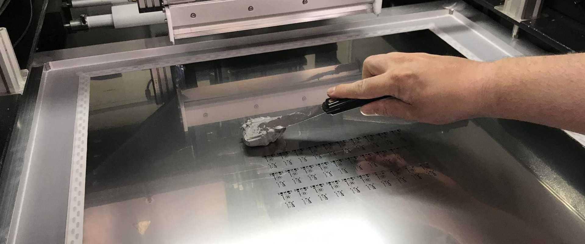
PCB Imaging
The circuit layout artwork must be accurately transferred to the laminate to form the conductive pattern. The main imaging methods are:
Photolithography
A photoresist coating is exposed to UV light through a mask with the layout pattern. After developing, the exposed image remains as an etch resist.
Direct Imaging
Lasers or ion beams are raster scanned to directly ablate away unwanted copper instead of using masks and chemicals. Higher resolution than photolithography.
Inkjet Printing
Conductive and resistive inks are deposited directly onto substrates. Suitable for specialized applications. Limited resolution.
For multilayer boards, the interlayer dielectric also goes through a similar imaging step to form the vias. The imaged panel then proceeds to etching.
PCB Layer Stackup
For multilayer PCBs, several etched single boards are aligned and bonded together with adhesive into a consolidated circuit:
Layer Preparation
Additional surface treatments promote adhesion like resin coating, oxide treatment, or chemical bonding.
Layer Alignment
Precision equipment aligns layers using optical markers or mechanical pin alignment. Alignment accuracy is critical for reliable interconnections.
Bonding
Layers are pressed together under heat and pressure. Adhesive is cured to create a permanent multilayer sandwich.
Inspection
Post-lamination inspection under x-ray or SONAR examines internal features to ensure no voids or alignment issues.
A similar layup process may be repeated several times for high layer count boards or boards with sequential-lamination.
PCB Drilling
Holes are created in the PCB to allow insertion of component leads and creation of vias between layers:
Drill Bit Selection
Bits matched to the hole size and material are selected. Multiple bits required for different hole sizes. Bits have limited life requiring frequent replacement.
Mechanical Drilling
CNC drilling machines use bits to bore holes. Spindles allow multiple bits for holes at varying pitches. Drill depth is precisely controlled. Debris is vacuumed during drilling.
Deburring
The edges of drilled holes are abraded to remove rough edges which could cut trace conductors.
Hole Wall Preparation
A plasma etch cleans the hole wall and roughens it for improved plating adhesion.
Drilling is a critical step impacting structural and electrical connectivity. Tight tolerances on hole location, size, shape, and wall quality must be maintained.
PCB Plating
Plating deposits the conductive elements onto the patterned laminate board:
Through-Hole Plating
All drilled holes are plated to form vias between layers. Electroless copper initially seeds the hole walls, followed by thicker electroplated copper.
Pattern Plating
After imaging, copper tracks are plated to desired thickness. Plating increases trace dimensions to final size. Often a nickel/gold finish is applied to exposed copper.
Edge Plating
Connector tabs or fingers along board edges receive plating to allow soldering or insertion into connectors.
A post-plating etching step will remove all unplated copper. Plating buildup defines the final conductor thicknesses on the PCB.
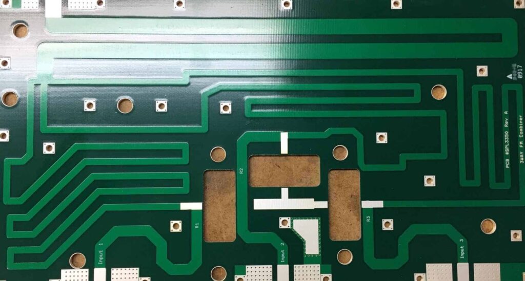
PCB Etching
Etching involves removing the unwanted copper which was not protected by photoresist or plating:
Wet Chemical Etch
A chemical bath dissolves away exposed copper while leaving the resist-protected areas intact. Multiple baths are used for high accuracy etching.
Dry Etching
Reactive ion etching uses a plasma to ablate copper in defined locations. Tight process control avoids over-etching. No liquid waste produced.
Etching defines the conductive pattern on the PCB while isolating traces from each other. Complete copper removal between conductors is vital to prevent short circuits.
PCB Solder Masking
A solder mask is a polymer coating which protects exposed copper from oxidation and prevents solder bridges:
Liquid Photoimageable Solder Mask (LPISM)
The most common method – a UV-sensitive polymer layer is imaged, exposed, and cured to form a permanent coating with openings only over solder pads.
Screen Printed Solder Mask
Liquified mask material is forced through a screen onto the board with openings in the desired locations. Less capable of fine features than LPISM.
Conformal Coating
Entire board surface is coated with a protective polymer. Selective coating at component pads done manually prior to coating. Not as advanced as LPISM.
Solder masks prevent shorts and must provide the required insulation, oxidation resistance, thermal, and mechanical properties.
PCB Silkscreen
Silkscreen printing applies epoxy-based ink markings onto the PCB to indicate component designators, polarity, board name, and other assembly details.
The markings guide manual and automated assembly operators. Accuracy of outlines, text, symbols, and alignment is important. Silkscreen tolerates some misalignment but overlaps cause obscuring.
Laser direct imaging allows changing silkscreen for each panel. Traditional methods use a fixed silkscreen pattern.
PCB Scoring and Depaneling
Fabricated boards are arranged in arrays on panels for mass manufacturing:
V-Cut Scoring
A rotating saw blade partially cuts the border between boards forming a V shaped groove. The residual web can then be broken after assembly to separate boards.
Tab Routing
Tabs are left connecting boards which hold them together during fabrication but are easily broken off later.
Edge Trimming
Individual boards have their edges trimmed to final dimension to remove any defects or roughness.
Careful scoring or depaneling prevents damage during separation into individual PCBs. Stubs or torn areas can impact reliability or assembly.
PCB Testing and Inspection
Testing during fabrication and after completion ensures quality:
First Article Inspection
The first board from a panel is thoroughly measured and inspected against specifications. This qualifies the process settings.
In-Process Inspection
Automated optical inspection (AOI) examines features like line widths, registration, etc. Statistical sampling may be used once qualified.
Electrical Testing
Continuity, resistance, and isolation are electrically tested. Some boards undergo dedicated functional testing.
X-Ray Inspection
X-ray imaging reveals hidden defects like voids in vias or plating. Especially useful for multilayer boards.
Frequent testing and inspection prevents defective boards from proceeding further and accumulating additional value-add processing.
PCB Assembly
After the bare boards are fabricated, electronic components are mounted and soldered to assemble the finished circuit:
Component Placement
Pick-and-place machines precisely position and orient components onto solder paste deposits. High speed capable for volume production.
Soldering
Reflow ovens melt solder paste to create reliable solder joints between pads and component leads or balls. Selective wave soldering used for through-hole parts.
Cleaning
Flux residue is cleaned. Components may be washed or cleaning done just around joints.
Programming/Functional Test
Microcontrollers, memories, or custom circuits are programmed. Complete functional test performed.
The quality of bare board fabrication impacts assembly yield and long term reliability in application. Comprehensive testing post-assembly provides final validation before shipment.
Key Factors in PCB Fabrication
Throughout the multilayer PCB fabrication process, some key factors influence the quality and performance of the finished board:
Registration Accuracy
Precise imaging, drilling, and stacking alignment enables conductors and holes to match across layers. Tight process controls and inspection required.
Etch Control
Complete copper removal leaving only intended conductors. No undercutting or over-etching. Chemistry, temperature, dwell times optimized.
Plating Quality
Uniform plating thickness across features. Good throwing power into holes with no voids. Minimal nodules or artifacts.
Lamination Pressure
Consistent pressure across layers removes air pockets and provides excellent bonding and stability.
Surface Finish
Good adhesion of subsequent coatings like solder mask relies on properly prepared substrate surfaces.
Hole Integrity
No barreling, no hole deformation, no lamination gaps around holes. High aspect ratio holes require special drill bits.
Cleanliness
Strict cleanroom protocols, laminar flow hoods, operator garments all protect boards from contamination.
Process Capability
Statistical analysis of process performance using Cp/Cpk metrics assures stability and reduces defects.
A deep understanding of materials science, chemicals, equipment, and manufacturing techniques is needed to master the intricacies of PCB fabrication.
Conclusion
The transformation of a PCB design into a high quality physical circuit board relies on proficiency in a series of complex fabrication processes. Each step integrates inputs, material handling, precision machinery, specialist skills, inspection, and testing technologies.
Optimizing the entire workflow from initial processing of raw laminate through drilling, plating, patterning, masking and assembly requires expertise and rigorous process control. As PCB technology advances to accommodate faster speeds, higher density, and new materials, staying current on manufacturing capabilities is key to harnessing innovations.
Frequently Asked Questions
What are some key differences between PCB prototype vs production fabrication?
Prototyping utilizes smaller volumes, more verification steps, and may permit different materials or looser tolerances than volume production which requires maximum efficiency and yield.
What fabrication methods are used for flex PCBs?
Flex PCBs use polyimide or other flexible substrates. Additional bonding steps laminate cover layers. Etching and drilling are adjusted for the thinner, flexible materials.
How is the fabrication process different for HDI PCBs?
HDI uses thinner dielectrics, greater stackup, smaller vias, and often direct imaging or laser drilling. It reduces capacitance for higher frequencies but demands tighter process control.
What role does automation play in PCB fabrication?
Automated optical inspection (AOI), material handling, and inventory management between process steps improves quality, throughput and traceability.
What are some key PCB fabrication quality certifications?
IPC standards validate PCB fabrication processes. ISO 9001 governs quality management. Cleanrooms follow IEST or ISO 14644 standards.


Leave a Reply