Introduction
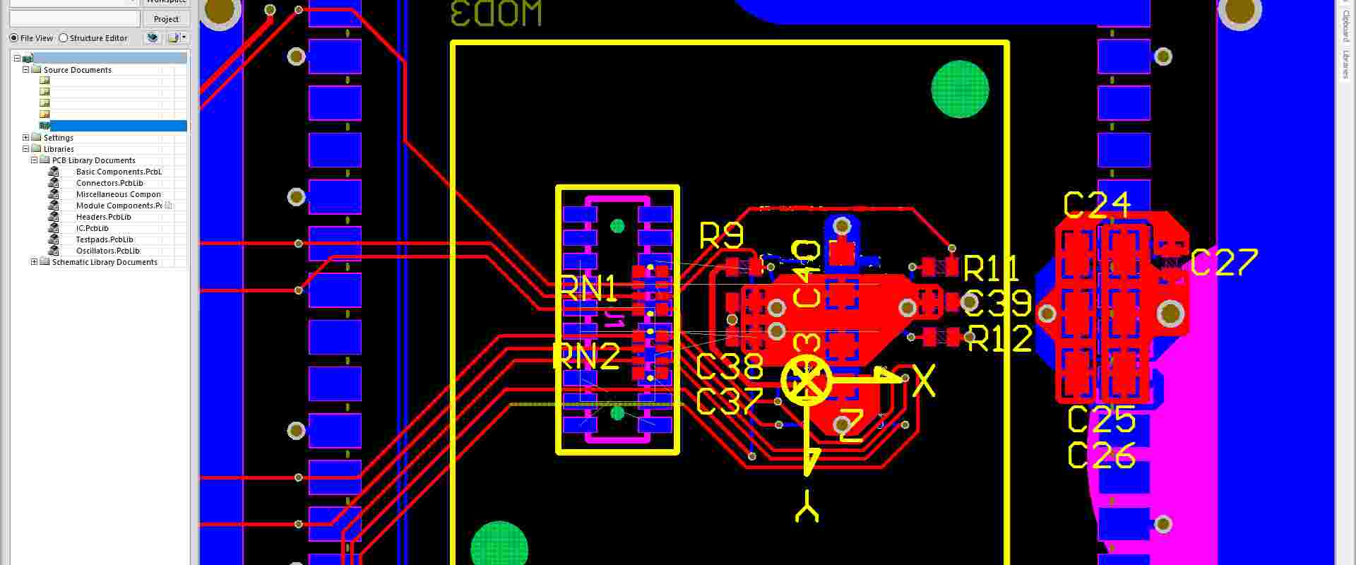
A PCB (printed circuit board) footprint refers to the pattern of copper pads and traces on a PCB that are used to mount and connect an electronic component. It provides both the physical mounting as well as the electrical connection for the component.
The footprint must match the specifications of the component so that it can be properly soldered and electrically connected to the PCB. It is a critical part of the PCB design process to ensure footprints are properly designed and laid out for each component on the board.
Some key characteristics of a PCB footprint include:
- The shape and dimensions of the pads
- Spacing between pads
- Number of pads
- Hole diameter for through-hole components
- Solder mask openings
- Silkscreen outline
In this comprehensive guide, we’ll explore what PCB footprints are in detail, the key elements that make up a footprint, how to design proper footprints, and review footprint libraries and how to manage footprints in your PCB design software.
What is a PCB Footprint Made Up Of?
A PCB footprint is made up of a number of elements that must be properly designed to match the specifications of a particular component. Here are some of the most common elements:
Pads
Pads provide the electrical connection as well as physical mounting for leads or terminals on a component. For through-hole components, pads will include a plated through hole. For surface mount devices, only a copper pad is required.
Pads must match the size and pitch of component leads or terminals. The shape can be round, oval, or rectangular. The dimensions must provide enough solderable area to establish a reliable connection without creating any risk of shorting between pads.
Silkscreen Outline
The silkscreen outline is a visible line printed on the surface of the PCB in the shape of the component’s profile. This allows placements of the component to be visually verified. Silkscreen is applied to both the top and bottom of the PCB.
The outline should provide clear visual reference for the body of the component. Keep in mind components may not be perfectly aligned with the outline so provide some clearance.
Solder Mask Opening
The solder mask is the protective coating applied to the PCB that leaves the copper pads exposed. The solder mask opening is area encompassing all the pads for that component with the proper clearance.
Sufficient clearance must be provided within the opening between the copper pad and solder mask to account for variances in the solder masking process. Typically a clearance of at least 0.05mm is recommended.
Assembly Outline
For some components, an assembly outline may be used to clearly show the extents of the component. This is useful for large components like connectors that cover a significant area of the PCB. It allows assemblies operators to easily find the placement area.
Polarization Indicator
For components like electrolytic capacitors or diodes that must be oriented in a certain direction, a polarization indicator is sometimes used. This can be an extra pad or modified pad shape that visually indicates the orientation.
Thermal Pad
Components like voltage regulators or LEDs that generate significant heat often required thermal pads. These provide a large exposed copper area to help dissipate heat into the ground plane of the PCB.
Fiducials
Fiducials are visual reference markers on the PCB that assist with component placement. They may be placed within the footprint to aid automated assembly machines.
Other Markings
Reference designators, component values, and other text markings are often included within the footprint to identify the component. These help assemble operators ensure the correct parts are placed.
Standard Footprint Types
There are many types of standard footprints used in PCB design corresponding to the different types of electronic components. Some common examples include:
Through-Hole Footprints
Through-hole components use leads or pins that go through plated holes in the PCB. Common examples are axial leaded resistors, ceramic capacitors, connectors, etc. The footprint consists of pads with holes arranged at the correct pitch for that component.
Surface Mount Footprints
Surface mount components are attached directly to the surface of the PCB with pads. There are many types of surface mount packages. Some common packages include:
- SOT – Small Outline Transistor
- SOP – Small Outline Package
- QFP – Quad Flat Package
- BGA – Ball Grid Array
The pads are arranged in the standard pattern for that package type at the recommended pitch. The dimensions and clearance are based on the datasheet recommendations to enable proper soldering.
Castellated Footprints
Castellated modules like QFNs or LGAs have pads along the edges of the underside. The footprint has an array of edge pads with the proper mask openings. Sometimes a thermal pad is incorporated.
Other Standard Footprints
Many other standard footprints exist for common package types like TO-220 transistors, 1206/0805 sized SMT components, DIPs, connectors, etc. Most PCB software includes libraries of the common industry standard footprints.
Considerations for Footprint Design
Here are some of the key considerations when designing footprints:
Datasheet Recommendations
Always refer to the component datasheet for detailed specifications on pads, pitch, solder mask openings, and other critical dimensions. Using the recommended dimensions ensures the part can be properly assembled and soldered.
Pad Dimensions
Make sure pads are large enough to allow sufficient solder volume and mechanical strength, but not so large they increase the risk of shorts.
Clearances
Provide sufficient clearance between copper pads and from the pads to solder mask openings and silkscreen. This accounts for tolerances in manufacturing and assembly.
Thermal Considerations
Make sure pads and openings provide adequate heat dissipation for high power parts. Incorporate large thermal pads where required.
Mechanical Stability
The footprint design must give the part sufficient mechanical stability. Through-hole pins provide stability. Some SMT parts may require glue or anchor points.
Ease of Soldering
The footprint should allow molten solder to easily flow across all pads during assembly. Make sure pads are not obstructed by mask openings or silkscreen.
Ease of Inspection
Provide sufficient opening in solder mask for electrical testing probes. Allow visual inspection of solder joints.
Polarization
Clearly indicate component orientation with polarized footprints. Make them visually asymmetric.
By carefully considering these aspects, you can design footprints that enable easy and reliable assembly. The goal is to match the physical footprint needed by the component as closely as possible.
Creating Footprints in PCB Design Software
Most PCB design software tools allow you to create custom footprints and add them to libraries. Here is a general workflow for footprint creation:
- Specify dimensions: Enter exact dimensions for pads, openings, silkscreen, etc. based on datasheet recommendations.
- Create padstack: Define the pad shapes, drill holes, mask openings, and other plated and non-plated features.
- Arrange pads: Place pads at the specified pitch and layout.
- Add silkscreen outline: Draw a component outline that provides visual reference.
- Add other markings: Include polarity marks, component value, reference designator, etc.
- Check clearances: Verify sufficient clearance between copper and mask openings.
- Generate 3D model: Create a simple 3D model for visualization (optional).
- Save footprint: Add footprint to custom library for reuse.
Most PCB tools like Altium Designer, Eagle, OrCAD, KiCad etc have detailed tutorials on their specific footprint creation process.
Managing Footprint Libraries
To facilitate reuse of footprints, PCB design software utilizes footprint libraries. Some ways to use libraries effectively:
- Store standardized company footprint libraries in a central location for common access
- Use consistent naming conventions for the library files
- Categorize footprints in the library by component type for easy browsing
- Include manufacturer part numbers and datasheet links if possible
- Avoid duplicating common industry standard footprints
- Setup revision control for footprint libraries to track changes
- Perform periodic audit of custom footprints vs datasheets
- Include footprint creation and modification procedures in your design guidelines
Careful management of the libraries is essential for maintaining design integrity as footprints are shared across multiple PCB projects and designers. Libraries with uncontrolled changes or inaccuracies can result in defective boards.
Generating Footprints from IPC Standards

The IPC, a global standards organization for the electronics industry, maintains a set of standards for PCB footprints. These include:
- IPC-7351 – Generic requirements for surface mount footprints
- IPC-7351A – Additional specifications for common SMT packages
- IPC-7351B – Guidelines for pad dimensions, openings, tolerances
Many PCB libraries leverage these standards to define starting footprints when the exact component datasheet is not available. However, the IPC recommendations are generic and designed to accommodate a wide range of component variances.
It is always advisable to refine the IPC footprints with specific data from the component manufacturer datasheet when possible. This will provide the optimal footprint design. But in the absence of component data, the IPC standard footprints can be better than a purely custom footprint.
DFM Checks for Footprints
To ensure footprints meet manufacturing requirements, PCB design rule checking (DRC) and design for manufacturing (DFM) checks should be performed. Some examples include:
- Minimum annular ring: Checks for sufficient pad overlap of drill holes
- Minimum solder mask web: Checks solder mask webbing between pads
- Minimum clearance: Checks copper to copper clearance
- Component clearance: Checks for sufficient clearance between components
- Courtyards: Checks component footprint is safely within courtyard boundary
- Solder mask expansion: Validates expanded openings do not intersect
- Missing solder mask: Finds pads with incomplete mask opening
- Missing paste masks: Validates paste masks openings on SMT pads
- Pad size checks: Confirms minimum pad dimensions for manufacturability
Running DFM analysis can reveal potential assembly issues related to footprint geometries. By addressing any errors or warnings early in design, it avoids costly mistakes discovered late in the prototyping stage.
Conclusion
In summary, the PCB footprint defines the physical interface for an electronic component to be reliably assembled and interconnected. Careful footprint design by matching component specifications, adequate clearances, and standardized dimensions enables repeatable soldering, inspection, and testing.
Management of footprint libraries and leveraging industry standards helps improve design reuse. Rigorous validation using DFM checks is essential to avoid issues during manufacturing. As PCBs grow continually more complex, thorough footprint planning is one of the key pillars of a robust design process.
Frequently Asked Questions
What is the difference between a footprint and land pattern?
The terms footprint and land pattern are sometimes used interchangeably. However, land pattern refers specifically to the copper pads, while footprint includes the complete set of printed layers (pads, silkscreen, soldermask, etc.) that allow mounting of the component.
How accurate do footprint dimensions need to be?
Footprint features like pad sizes and spacing should match component datasheet recommendations as closely as possible, with tolerance of ±0.005 mm. This ensures proper soldering and reliability.
Can I use the same footprint for multiple components?
If multiple components have identical specifications for pads, pitch, holes, etc. then a single footprint can be reused. But always double check the datasheets thoroughly.
What is the best way to name footprint files?
Use a consistent naming convention like “Manufacturer-MPN-Package” e.g. “Microchip-ATmega328P-TQFP”. Some also include pitch and pad count.
How can I find the right footprint for a component?
Refer to manufacturer datasheet first. Then search trusted component supplier and PCB software footprints libraries. IPC standards can provide generic starting point.


Leave a Reply