A PCB (printed circuit board) library is a collection of footprint models used in PCB design software to represent real-world components. It contains 3D models and footprint patterns for components like resistors, capacitors, integrated circuits, connectors, etc. PCB libraries allow circuit designers to easily place components on a PCB layout by selecting from a list of available parts. The library handles the intricate details of each component’s physical dimensions, shapes, and pinouts so designers don’t have to create footprints from scratch. PCB libraries play a crucial role in simplifying and accelerating the PCB design process.
Why PCB Libraries Are Needed
Without PCB component libraries, circuit board designers would have to manually draw the outline, pads, holes, silkscreen, etc. for every part used. This would be extremely laborious and time consuming, especially for complex components like BGA packages or processors with hundreds of pins. PCB libraries automate this process by providing pre-made footprints that can simply be placed on the board layout. This saves engineers countless hours of effort compared to making footprints manually.
Some key reasons why PCB libraries are an essential part of the design workflow:
Streamlines PCB Design Process
PCB libraries allow engineers to select components from a list and place them directly onto the board layout, without any footprint drawing required. This significantly speeds up the PCB design process and allows faster iteration.
Reduces Errors
Manually creating footprints leaves room for human error in getting dimensions or pinouts wrong. Pre-made footprints eliminate this risk by providing accurate models designed to manufacturer specifications.
Enables Design Reuse
Once a component footprint is made once, it can be reused over and over in future designs rather than recreating it each time. This improves consistency and efficiency.
Facilitates PCB/Schematic Integration
PCB footprints include a symbol view that links to the schematic component for cross-probing between schematic and PCB. Libraries integrate these two domains.
Stores Manufacturer Data
The component models include manufacturer part number data and parametric information for procurement and manufacturing handoff.
Allows Component Interchangeability
Different manufacturers may make compatible components with the same functionality but slightly different parameters. Libraries enable swapping these interchangeable parts easily.
For these reasons, PCB libraries are an indispensable part of any PCB design flow to maximize efficiency and reduce errors. The availability of component libraries literally makes or breaks the ease of a particular PCB tool. Modern tools come bundled with extensive component libraries, and many provide open libraries for community contribution.
Types of PCB Libraries
While all PCB libraries contain pad and pin information to create footprints, there are different categories of libraries for different stages of the design process:
Symbol Libraries
Symbol libraries contain just the schematic symbols representing components logical connectivity. They are used when creating the schematic diagram to select parts and wire them together. Symbol libraries typically include graphical symbols, pins, part numbers, and sometimes parametric data.
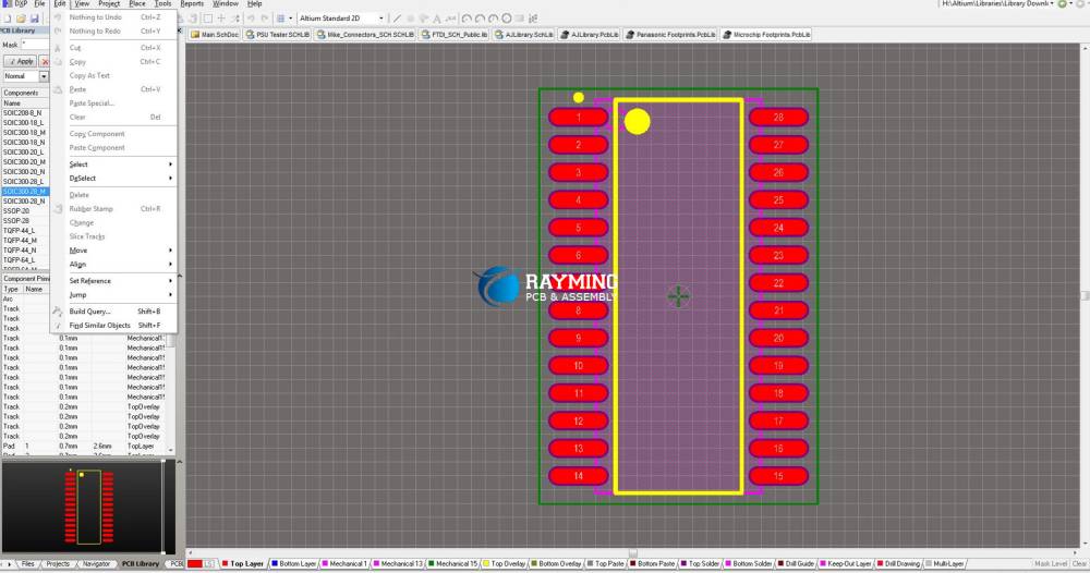
Footprint Libraries
Footprint libraries contain just the PCB footprint models of components without any schematic linkage. They are used in the PCB layout stage for placing components based on their physical land patterns. Footprints include pad stacks, lines, arcs, keepout areas, text, and 3D models.
Unified Component Libraries
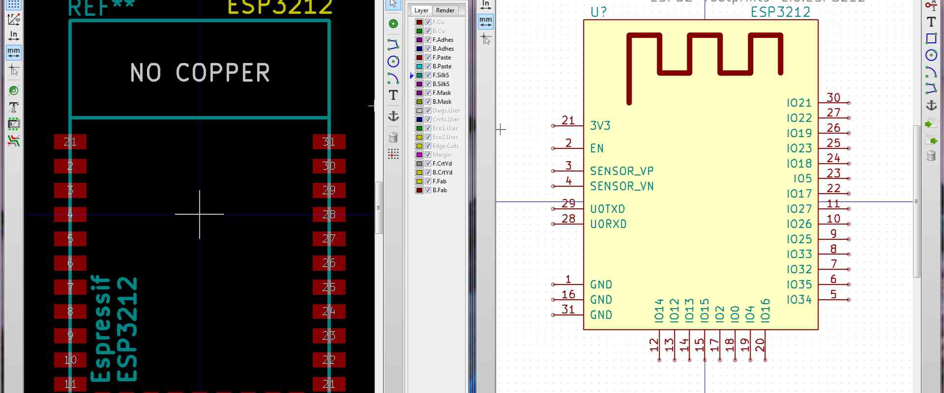
Unified or integrated component libraries contain both the schematic symbol and PCB footprint views of components in a single package. This allows cross-linking of logical and physical representations of each part through a shared part ID. Unified libraries power design synchronization and cross-probing between schematics and PCB.
3D Model Libraries
3D model libraries contain additional detailed 3D component models used for visualization, collision checking, and manufacturing outputs like mechanical drawings. These are supplemental to the simplified 3D models integrated into footprint libraries.
In general, unified component libraries with symbol, footprint, and 3D model integrally linked are the most efficient for streamlining PCB design and enabling optimal ECAD/MCAD collaboration. Leading PCB tools place strong emphasis on unified libraries and provide extensive library content.
Anatomy of a PCB Footprint
While schematic symbols visually represent logical connectivity, PCB footprints are physical pad patterns that correspond to the physical component. Here are the typical elements that make up a footprint:
Pads
Pads, or padstacks, form the electrically conductive areas that component leads or pins are soldered to. Pad geometry, dimensions, spacing, and layout precisely match the physical component. There are different pad types including SMT (surface mount), TH (through-hole), and hybrids.
Lines and Shapes
Lines, arcs, and other shapes create the outline of the component footprint defining its exact physical size and extent. The outline may include cutouts if present in the real component.
Silkscreen
Silkscreen lines and shapes are used to indicate component orientation, pin 1 location, component value text, and other annotations. These print on the PCB silkscreen layer.
Drills
Drilled holes are used for leads on through-hole components and may include properties like hole size, plating, etc. Some footprints may not use drills.
Text
Reference designators, value text, and other annotations are added as text objects associated with the footprint. These facilitate Bill of Materials generation.
3D Model
A simple 3D model of the component is integrated into the footprint. This adds visual information about height and component type to the 2D pattern for PCB profiling.
Courtyards
Courtyard outlines indicate minimum spacing needed around component for manufacturing, assembly, and service. This guides PCB layout and component placement.
Together, these attributes fully define both the electrical connectivity and physical space requirements for a component. Well-constructed PCB footprints make component placement very straightforward by automating the intricate details needed for manufacturing outputs and assembly.
PCB Library Creation
How exactly are component libraries built in the first place? There are generally two approaches:
PCB Tool Vendor Libraries
Most PCB design software packages come pre-bundled with thousands of ready-made component libraries. Vendors create these libraries to facilitate design for their users. Library content may include both common generic parts as well as vendor-specific components. These professionally developed libraries enable designing right out of the box.
User/Third-Party Libraries
Beyond vendor-supplied content, users can create custom libraries for any components needed that are not already covered. Some PCB tools include library editors, or libraries can be contracted out. User groups and third parties also develop and sell custom libraries. Building accurate component models requires manufacturer datasheets and mechanical drawings.
Parametric Libraries
More advanced than static libraries are parametric component generators that algorithmically produce footprints and 3D models based on user input dimensions and component specifications. These allow flexible generation of customized footprints tailored to requirements.
Whichever libraries are used, accuracy is essential for the PCB design process. Manufacturers provide component datasheets and 3D models to enable library developers to capture precisely correct physical parameters and pinouts needed for interoperability. The best libraries are validated through prototyping and fabrication testing.
Typical PCB Library Content
A full-featured PCB library contains thousands of component footprints across all common component types and categories. Here is a high-level overview:
Passives
- Resistors, capacitors, inductors in the full range of case sizes, styles, and form factors
- Networks/arrays for multi-unit packages
- Fuses, thermistors, varistors, beads
Actives
- Diodes, transistors, thyristors
- IC packages – DIP, SOIC, QFP, BGA etc. in all sizes with multiple pad configs
- LEDs in all shapes, sizes, and pinouts
Connectors
- Board-to-board, board-to-cable in standard pin counts
- Common interfaces: USB, Ethernet, HDMI, DVI
- Edge card, DIN, circular, terminal strip
- RF connectors like SMA, SSMA
Electromechanical
- Switches, relays, terminals, test points
- Common components: buttons, buzzers, fuse holders, battery holders, etc.
Miscellaneous
- Transformers, chokes, inductors, ferrites
- Crystals, oscillators, resonators
- Hardware pieces: standoffs, screws, nuts, rivets, clips
- Graphics/logos, fiducials, markers
The most inclusive libraries contain thousands of validated components in each category to enable maximum selection. Extensive generic libraries coupled with device/vendor-specific parts offer the full spectrum for PCB design.
Beyond this generic content, any custom or uncommon components needed can be added through user library creation or parametric footprint generation.
PCB Library Management Best Practices
Careful management of PCB component libraries is crucial for maintaining efficient design workflows. Here are some key organizational and maintenance practices for libraries:
Logical Organization
Libraries should follow a logical hierarchical structure that matches typical component groupings by type/function rather than just an alphabetical sequence. This aids part browsing and discovery during design.
Standard Naming Conventions
Establishing and following consistent naming conventions for library elements helps keep libraries orderly as they grow. Descriptive but short names work best.
Database Integration
The best library structures utilize relational databases rather than flat file folders to enable powerful filtering, querying, and reporting across large library contents.
Revision Control
Maintaining libraries under version control enables tracking edits, attributing changes, and roll-back when needed to a prior version. This aids stability and collaboration.
Documentation
Comprehensive documentation on structure, naming, revisions, and change log helps keep libraries maintainable over time as multiple users interact with them.
Clean-Up and Audit
Periodic auditing to fix errors, delete unused or obsolete libraries, consolidate redundancies, etc. keeps libraries lean and efficient over time.
User Access Controls
Establishing proper permissions and access controls prevents unwanted changes and facilitates team-based libraries.
Following these practices helps facilitate large, shared libraries that evolve constructively over time through contributions from multiple PCB designers. Library organization has a major impact on designer productivity.
PCB Libraries for Manufacturability
Beyond just the electrical connectivity that allows PCB layout and routing, component footprints also communicate physical design intent for manufacturing and assembly. The footprint geometry represents the space claim of the component on the board such that the PCB factory output matches the intended design.
Some key considerations for how libraries interface with manufacturing:
Footprint Accuracy
Footprint pads, outlines, and spacing must precisely match component datasheet specifications to ensure manufacturability. Tolerances are tight, especially for ultrafine pitch components.
3D Clearances
3D component models interact with board topology to validate clearances for assembly and service. Maximum component height data aids clearance analysis.
Courtyard Guidelines
Courtyard spacing in libraries provides assembly workers clear space for part placement. These margins also facilitate cleaning, inspection, and rework if needed.
###Pick-and-Place Data
Libraries contain center of mass information, rotational limits, and other pick-and-place assembly data exported through manufacturing documentation.
Solder Process Data
Libraries specify thermal pad sizes, paste masks, and other soldering parameters to inform solder process development for reliable assembly.
Component Metadata
Libraries contain supplier identifiers and component descriptions which link to procurement for bill of materials accuracy through manufacturing.
PCB fabricators rely extensively on component library data to translate design intent into high-quality physical boards. Complete component models in libraries are crucial for first-time-right manufacturing outputs.
The Future of PCB Libraries
PCB component libraries continue to evolve with the advancing capabilities of ECAD tools and library formats. Some trends in PCB library innovation include:
Cloud Libraries
Cloud-based library platforms enable unified access to component data across design teams and global locations. Web accessibility also eases third party contributions.
Data Automation
Web scraping, AI, and machine learning are being leveraged to automate data mining from manufacturer websites to accelerate library creation and updating.
Digital Twins
Digital twin bridge models integrate component simulation data for virtual prototyping of PCB performance based on real-world library models.
Model Reuse
Libraries are moving towards reuse of high-fidelity 3D component models from MCAD tools for integrated ECAD/MCAD design collaboration.
Version Control
Advanced version control systems provide detailed library change management, branching, and exploration of design alternatives.
Smart Search
More advanced search, filtering, and classification of component data improves library navigation and component discovery.
As PCB design scales in complexity, libraries must evolve to provide greater accuracy, connectivity, and design-manufacturing integration. The role of next-generation library management is making components easy to find, integrate, analyze, build, and procure. Component libraries sit at the heart of the PCB design flow.
Frequently Asked Questions
What are the main differences between schematic and PCB component libraries?
The key differences are:
- Schematic symbols represent logical connectivity while PCB footprints represent physical shape and space requirements.
- Symbols focus on pins and part numbers while footprints focus on pads, outlines, text, and 3D models.
- Symbols link to device behavior models while footprints link to physical parametric data.
- Symbols enable schematic capture connectivity while footprints enable physical PCB layout.
Though different in purpose, integrating common part identifiers allows cross-probing between logical and physical views in a unified component library.
How do I know if a component library footprint is of good quality?
Characteristics of quality library footprints:
- Dimensions precisely match datasheet measurements
- Pad geometries/spacing follow IPC guidelines
- Silkscreen indicates pin 1, orientation, component value
- Courtyard provides safe assembly margin
- 3D model represents visual height and body details
- Contains complete metadata – part number, description, parameters
- Verified through comparison, testing, and prototyping
The best libraries utilize manufacturer 3D models coupled with extensive validation to ensure footprints produce functional boards.
Can PCB footprints be modified if needed during layout?
Yes, most PCB tools allow editing or overriding footprint properties as needed during board layout while keeping the original library footprint unchanged. Typical edits are to pad geometries, text values, courtyard spacing, or 3D model orientation. The ability to tweak footprints on-the-fly provides flexibility while retaining library consistency. Edits should be carefully validated.
How are custom or uncommon component footprints added to a library?
Typical approaches to create new custom footprints:
- Build from scratch in library editor tool using datasheets
- Modify existing footprint to match target component
- Use parametric generator to tailor footprint to specifications
- Contract out to component library service providers
- Contact manufacturer for 3D model and footprint details
- Reverse engineer from measurements of physical component sample
Adding new parts is easiest using datasheet dimensions or by editing similar existing footprints. Verification through testing is key to ensure functionality. Libraries are designed to be extended with custom components where needed.
If different PCB tools use differing file formats, how are libraries shared?
Most PCB tools can import/export libraries in standard interchange formats like:
- IPC-7351 – Generic CAD footprint format
- ODB++ – Assembly data standard
- STEP – 3D model standard
These standards allow exporting library data from one system and reliably importing into a different tool with component integrity maintained. Vendors also provide direct library converters between popular tools.
So in summary, mature library standards enable transferring libraries between multiple PCB systems via export/import or conversion while retaining all model intelligence. Library portability facilitates data sharing.
Conclusion
PCB component libraries are collections of schematic symbols and PCB footprints enabling rapid placement and routing during board layout. Well-constructed libraries eliminate the need to recreate component footprints over and over. Libraries therefore play an indispensable role in simplifying PCB design and enhancing engineering productivity.
Libraries bridge the gap between logical schematic connectivity and physical layout by integrating symbols with matched footprints into unified component models. They automate the intricate details of shape, spacing, and dimensions for each part represented. PCB designers rely extensively on component library completeness and quality to transform concepts into manufacturable boards efficiently.
Looking ahead, continued improvements in standards, modeling sophistication, and data connectivity will further enhance the capabilities of PCB libraries. The evolution of component library management and accessibility will be a key driver of next-generation electronics design. Component libraries sit squarely at the foundation of seamless ECAD to MCAD collaboration and integrated manufacturer design flows.


Leave a Reply