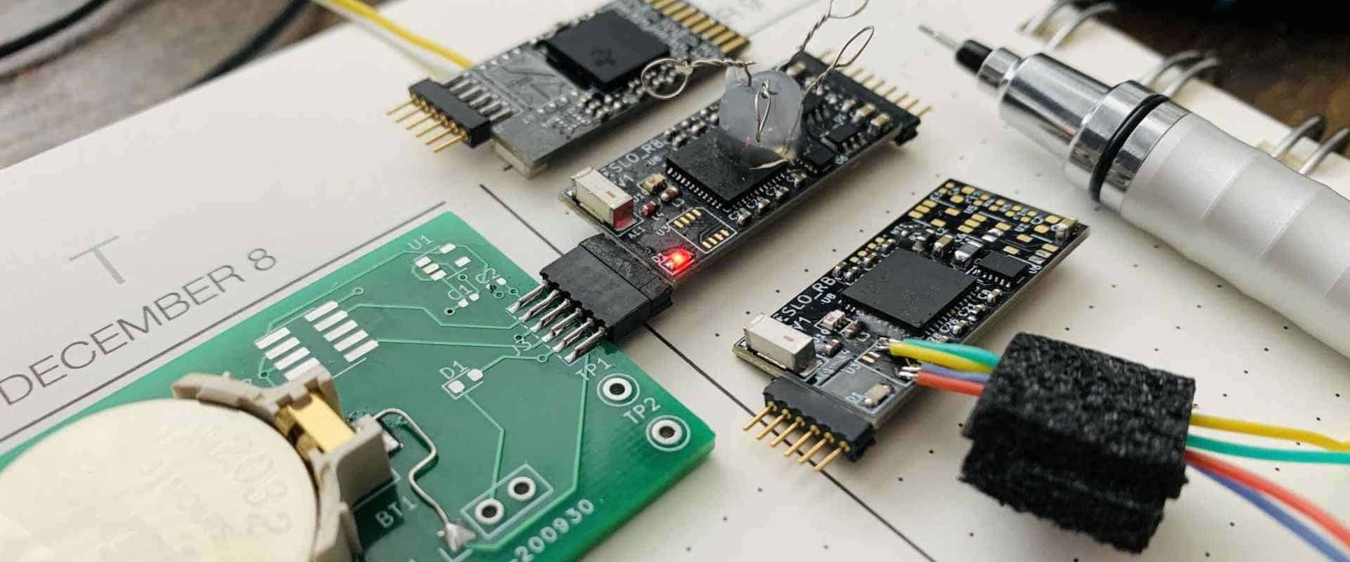
Introduction
Reverse engineering of printed circuit boards (PCBs) involves analyzing an existing board to determine its design, components, and functioning without access to the original schematics or layout files. It is useful for extracting design data from old legacy boards, studying competitors’ products, or debugging equipment issues. While challenging, skilled engineers can deduce PCB design through methodical deconstruction, measurement, testing and documentation.
This guide covers key techniques and best practices for systematically reverse engineering PCBs.
Safety Precautions
Take appropriate precautions when handling boards to avoid damage or injury:
- Use anti-static mat and ground bracelet when handling bare boards
- Power down and discharge stored voltages before working
- Check for components with high voltages or power levels
- Be careful around likely fuse or fault areas
- Follow ESD safe procedures to avoid damaging boards or components
Initial Visual Inspection
Start with visual examination of the board’s physical attributes:
- Note board dimensions, layer count, materials, weight and finish
- Identify components types, values, markings and package sizes
- Check for unpopulated footprints or unused connectors
- Look for areas with repaired/replaced components or damage
- Note shielding, silkscreen labels, testpoints and any markings
- Flag any unidentified components or sections
Thorough visual inspection will reveal much about the board’s functionality and technologies used.
Non-destructive Testing Techniques
Use these techniques initially for analysis without directly modifying the board:
X-Ray Imaging
X-ray imaging can generate images of inner board layers and identify hidden components.
Ultrasonic Scanning
High frequency sound pulses can locate faults like cracks or delamination.
Thermal Profiling
Infrared scanning during operation visualizes hot spots on the powered board.
Emissions Probing
Monitoring electromagnetic emissions can map signals and high frequency trace paths.
Edge Connector Testing
Test points at board interfaces can be used to sniff signals and trigger events.
Power-Up Testing
Apply limited power and probes to map basic board operation.
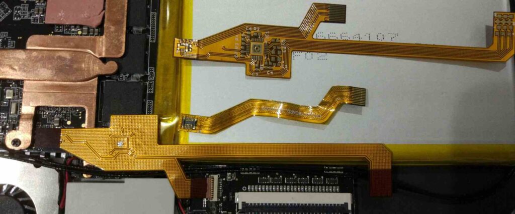
PCB Layer Separation
To access inner board layers, carefully separate the board:
- Use a thin, heated knife to slowly slice layers starting at the edge
- Keep the temperature moderate to avoid charring the laminate
- Split ground/power planes along score lines scored with utility knife
- Remove stubborn layers with delicate prying or by reheating
- Photograph each layer as it gets exposed for documentation
Separating layers provides valuable insights but destroys the board. Use sparingly on less critical areas.
Trace Mapping
Reconstructing interconnects is key to generating a board schematic. Trace mapping approaches include:
Manual Tracing
Literally follow copper traces node-to-node with visual inspection, noting connections.
Probe Tracing
Use multimeter probes to trace conductivity between points to map nets.
Microscope Probing
With high magnification, gently probe fine traces to determine connections.
Chemical Etching
Selectively etch copper briefly to reveal covered traces connecting between vias.
X-Ray Inspection
X-rays can show underlying traces and vias within outer layers.
Thoroughly map all visible trace interconnects and interfaces on the board.
Identifying Components
Determine part numbers and specs for all components:
- Note package type, markings, size to find datasheet
- Look up any coded part numbers
- Remove a subset of parts for closer inspection if uncertain
- Match to reference design libraries by appearance
- Consult BOMs from similar boards as a clue
Any failed or suspicious parts may require replacement for further testing.
Understanding Circuit Functions
Analyze board sections to infer their functions:
- Separate analog and digital sections based on identified components
- Processor and support logic will be discernible
- Look for discrete hallmarks like oscillators, filters, amplifiers, etc.
- Follow power, ground traces to likely high current sections
- Match RF layout shapes to antenna, mixer, filter building blocks
- See if areas can be powered up independently
Leverage identified components, layouts and PCB zones to deduce circuit functions.
Powering Up The Board
Cautiously apply power for functional testing:
- Attach temporary clip or connector leads
- Power up with current-limited bench supply
- Gradually increase voltage while monitoring signature
- Check for shorts, excessive heating, oscillator activity
- Probe around powered components to map data flows
- If possible, stimulate inputs to verify outputs
Powering sections separately helps isolate board functions for analysis.
Capturing the Schematics
Translate the reverse engineering observations into schematic documentation:
- Create parts list from identified components
- Lay out parts corresponding to board orientations
- Add traced interconnects between sections
- Assign functional blocks based on circuit types recognized
- Designate key interfaces, testpoints, connectors
- Identify data and control buses between components
- Label power and ground domains
- Find possible points for debugging access
Generating schematics helps understand key design aspects and interactions for reverse engineering goals.
Applications of PCB Reverse Engineering
Reverse engineering provides useful insights for many applications:
- Understand old circuits from obsolete boards no longer manufactured
- Enable maintenance and repair of equipment when designs are unavailable
- Discover undocumented features or performance enhancements
- Assess vulnerabilities or extract sensitive data remnants
- Qualify authentic components vs counterfeits
- Troubleshoot assembly issues or product field failures
- Derive design rules and constraints for cloning purposes
- Violate patents, copyrights or intellectual property protections
- Analyze competitor designs for performance comparisons
- Identify opportunities for upgrades, accessories or revisions
The process requires meticulous inspection, testing, analysis and documentation. Legal and ethical issues regarding rights to intellectual property must also be considered.
Challenges of Reverse Engineering PCBs
Reverse engineering has limitations and risks:
- Missing schematics or BOM information leads to uncertainty
- Difficulty tracing obscured interconnects within layers
- Components may be damaged during deconstruction
- Powering the board could cause latent damage
- Complex ICs may have inaccessible proprietary contents
- Analysis requires specialized skills and equipment
- Time required to reproduce the full design can be extensive
- Legal restrictions apply against IP theft of copyrighted material
Thorough planning is required to balance these factors and achieve useful reverse engineering results.
Conclusion
Reverse engineering provides valuable insights into the design, functionality and composition of electronic systems by systematically analyzing an existing PCB. While time consuming and technically challenging, skilled engineers can deduce key design elements through careful visual, electrical, and chemical analysis of boards layered contents and components. Important techniques include visual inspection, layer separation, probe-based net tracing, power up testing, and function analysis. By properly documenting the findings, PCB reverse engineering allows recovering design data, facilitating repair and upgrades, studying competitive products, and troubleshooting field failures.
Frequently Asked Questions
What are some key steps in the PCB reverse engineering process?
- Visual inspection of board
- Non-destructive probing and emissions analysis
- Safe layer separation as needed
- Mapping tracings and nets
- Identifying components and their functions
- Powering up sections and testing
- Reconstructing schematics
What types of information can be obtained by reverse engineering PCBs?
The components used, board materials, layer stackup, trace interconnects, net names, functional blocks present, data flows, power distribution, high-speed routing, board dimensions, and connector interfaces can typically be deduced.
What risks are involved in reverse engineering PCBs?
Beyond component damage, there are risks of electrical shorts and latent physical damage from improper handling. Reproducing protected intellectual property also carries legal liability.
What tools and skills are most important for PCB reverse engineering?
A multimeter, magnifying glass, soldering iron, knife, and chemical etchants are essential tools. Strong electrical, PCB layout, rework, and analytical skills are needed.
How can reverse engineering PCBs save time versus original schematic design?
By leveraging existing proved, functional board layouts and component choices, the time to recreate schematics and PCB footprints from scratch can be reduced greatly.


Leave a Reply