Introduction
A PCB antenna is an antenna constructed using the same laminate material and manufacturing processes used for printed circuit boards (PCBs). Instead of or in addition to copper traces, the PCB contains carefully shaped copper antenna elements on one or more layers to radiate and receive electromagnetic waves.
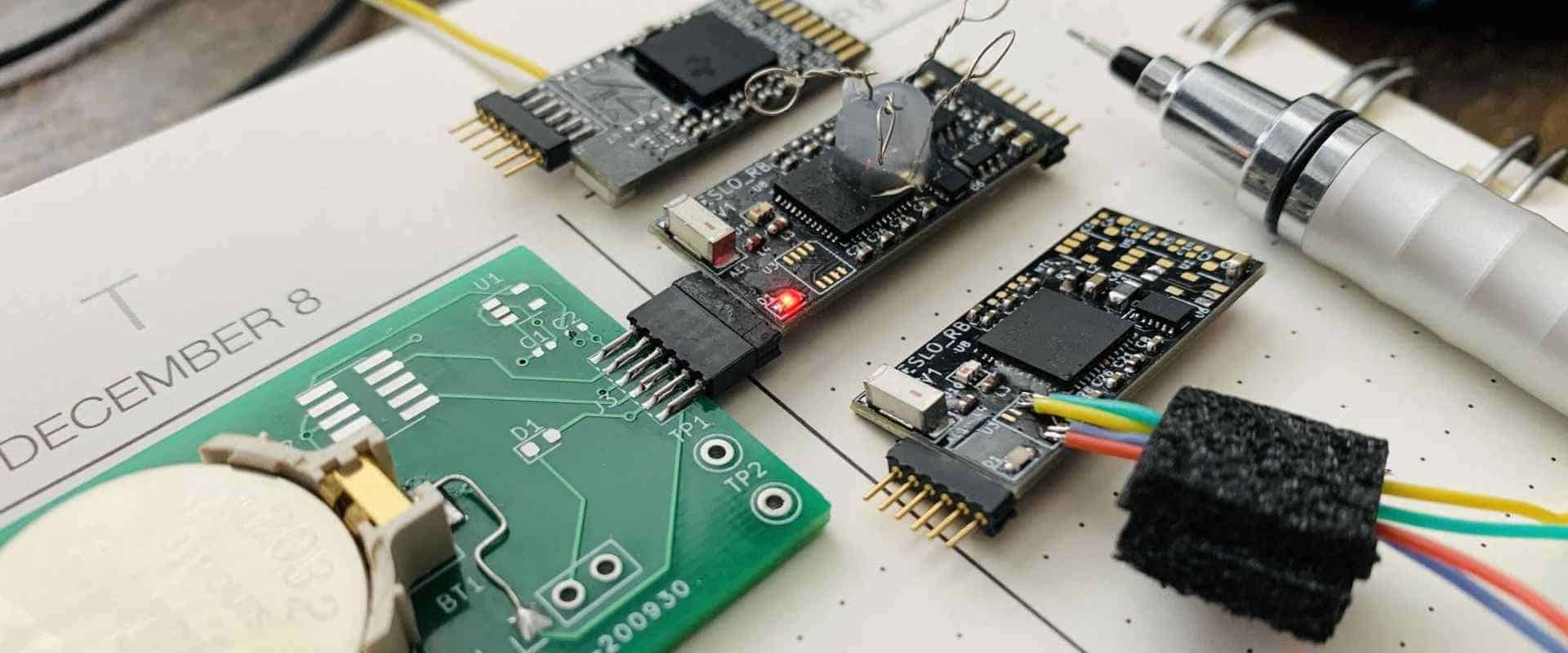
PCB antennas integrate the antenna directly into the circuit board, eliminating the need for an external antenna. This saves space, cost, and assembly steps. PCB antennas are found in many wireless electronic devices including phones, tablets, IoT devices, routers, automotive electronics, and more.
This article provides an in-depth overview of PCB antenna technology, designs, performance factors, applications, and tradeoffs. We’ll look at how PCB antennas work and the benefits they provide compared to other antenna types.
How PCB Antennas Work
PCB antennas contain copper antenna elements etched into the board that are shaped to efficiently convert conducted electrical signals into radiated electromagnetic waves and vice versa. The elements act as resonators, tuned to oscillate at the operating frequency.
The antenna elements couple energy to/from the electromagnetic field. The board substrate forms the antenna dielectric. Exact antenna geometry shapes the radiation pattern. Just like transmission lines, antennas are optimized for the dielectric type and thickness.
Microstrip patch, planar inverted F, and monopole type designs are common. Via fences, keepouts, and ground planes help shape the patterns. Just as circuit traces route signals on a PCB, antenna elements route energy to/from free space radiation.
The integration of antennas and circuits into a single PCB platform enables high performance wireless systems in a compact footprint. Let’s look further at the benefits PCB antennas offer.
Benefits of PCB Antennas
There are several compelling reasons to select a PCB antenna rather than a traditional external antenna:
Size – PCB antennas can take up far less space than external antenna modules. This enables smaller wireless device designs.
Cost – Eliminating connectors, cables, and discrete antennas reduces bill of materials cost and assembly expense.
Reliability – Fewer interconnects means greater reliability. Antennas fabricated into the PCB have less potential for defects and failures.
Efficiency – Better impedance matching and lower losses result from integration of antennas directly into the PCB substrate.
Reproducibility – The consistency and precision of PCB manufacturing results in repeatable antenna performance.
Design Flexibility – PCB antennas enable greater flexiblity in designing compact antennas tuned for the product requirements.
Aesthetics – Removing external antennas leads to a streamlined, integrated product appearance.
For many wireless products, the benefits clearly justify selecting a PCB antenna design.
Types of PCB Antennas
There are several common types of antennas that are frequently implemented on PCBs:
Microstrip Patch Antennas
Microstrip patch antennas are one of the most widely used types of PCB antennas. As the name suggests, these are planar antennas fabricated using PCB microstrip technology.
Patch antennas consist of a rectangular or other shaped copper patch suspended above a ground plane. The patch is fed using a copper transmission line with a connection point optimized for impedance matching. The surrounding ground plane isolates the patch element.
Patch antennas are low profile, inexpensive to manufacture, and integrate easily with microstrip circuitry. Drawbacks include narrow bandwidth and low gain. Patches can be used in arrays to improve gain and support polarization diversity.
Monopole Antennas
A monopole antenna contains a single straight copper antenna element, typically a quarter-wavelength long at the operating frequency. One side is connected to the transceiver, while the other extends out parallel to the ground plane.
The return current flows through the ground plane back to the feed point. Monopoles provide an omnidirectional radiation pattern. The ground plane size influences the pattern shape and gain. Monopole PCB antennas are very simple to implement.
Dipole Antennas
Dipole PCB antennas contain two symmetric copper antenna elements oriented end to end, with a small feed gap between them in the middle. Each pole is a quarter wavelength long. The elements are aligned perpendicular to the ground plane.
A balun is often needed to convert the balanced feed to an unbalanced coax interface. Dipoles have a bidirectional radiation pattern. They are easy to design and fabricate using standard PCB processing.
Planar Inverted F Antennas (PIFA)
The planar inverted F antenna gets its name from the shape of its main radiating element. A PIFA has a rectangular plate element connected to a perpendicular shorting plate that attaches to the ground plane below. There is a small feed gap in the bottom edge.
PIFAs provide good performance in a compact size, but have narrow bandwidth. The design can be tuned by adjusting the element size, feed point, and ground plane clearance. PIFAs are among the most common PCB antennas.
Loop Antennas
Loop or coil antennas contain a looped copper trace, often circular or square shaped. For PCB designs, the loop may be etched on the outer layer, embedded between layers, or implemented vertically using plated through holes.
Loop antennas are resonant antennas, with the circumference determining the operating frequency. Loops have high near-field coupling but small radiation resistance. Ferrite material may be added to increase gain.
There are many other specialized PCB antenna types, but the ones above represent most implementations. The choice depends on the needs of the particular wireless system and product.
PCB Antenna Performance Factors
Many factors determine the performance characteristics of a PCB antenna. Here are some of the most important design considerations:
Operating Frequency
The operating frequency influences antenna size and geometry. Lower frequencies require larger antenna structures. Traces and elements are sized based on the wavelength. Matching networks must provide the correct impedance over the frequency range.
Substrate Parameters
The dielectric constant and thickness of the PCB substrate affect the antenna dimensions and signal velocities. Low-loss, consistent dielectrics enable higher performance and efficiency. Common PCB laminates like FR4 can limit high frequency operation.
Copper Thickness
Thicker copper with higher conductivity reduces ohmic losses, improving quality factor and efficiency. But skin effect limits benefit above ~0.5 oz thickness. Balancing cost vs performance determines optimal copper weight.
Ground Plane
The size and placement of the ground plane shapes the radiation pattern. A large ground plane tends to result in more directional upward radiation. Small ground plane gives quasi-omnidirectional patterns. Proximity also affects coupling.
Element Shape
The physical geometry, length, width, angles, and bends of the antenna elements all influence the radiation pattern shape. Simulation is used to optimize shapes for directionality or polarization properties.
Matching Network
Impedance matching networks transform the antenna feed point impedance to match the system characteristic impedance, usually 50 ohms. Bad matching hurts efficiency. Tuneable matching allows dynamic optimization for changing conditions.
Feeding Method
The antenna feed arrangement strongly influences performance. Methods include microstrip, coaxial, aperture coupled, proximity coupled, and coplanar waveguide feeds. The feed location also affects matching.
Stackup Structure
Parameters like substrate thickness, layer count, stack ordering, laminate materials, and vertical interconnects impact antenna gain pattern, efficiency and bandwidth. Embedded elements can shape patterns.
By optimizing all these factors, PCB antennas can achieve excellent efficiency and gain for a given application compared to traditional antennas.
PCB Antenna Design Process
Antennas transform conducted electrical signals into radiated electromagnetic waves. The antenna geometry determines the transformation properties. This makes antenna design an exercise in shaping geometry to obtain desired gain patterns, tuning, and impedance characteristics. Here is the typical PCB antenna design flow:
1. Define Requirements
The design starts by identifying the key system and antenna requirements:
- Frequency bands
- Radiation pattern shape
- Polarization options
- Gain and efficiency needs
- Impedance and voltage standing wave ratio (VSWR) specs
- Size constraints
- Aesthetics
2. Select Antenna Type
Next, the antenna implementation is chosen based on requirements. A patch, monopole, dipole, PIFA or other antenna type that can likely meet the needs is selected as the starting point.
3. Model and Simulate
Model the antenna geometry and surrounding PCB features in 3D EM simulation software. Then simulate the model to analyze impedance, gain, efficiency, and radiation patterns over the desired frequencies.
4. Refine Design
Iteratively refine the layout by tweaking dimensions, shapes, feed location, ground planes, and other parameters to optimize the simulated results for the system needs.
5. Prototype and Validate
Build PCB prototypes and use network analyzers and anechoic chambers to validate the simulations, optimizing further as needed until the performance goals are met.
6. Finalize Design
Finalize board layouts, fabrication notes, assembly instructions, and performance specifications to handoff for production. Perform design reviews, DFMEA, safety certifications, etc.
Skilled antenna designers use established designs and extensive simulation and prototyping to develop new antenna geometries optimized for the product needs.
PCB Antenna vs Traditional Antennas
Traditionally, electronic devices use external antennas – discrete components connected to the PCB using connectors and coaxial cables. While still common, external antennas have some drawbacks compared to PCB integrated antennas:
| Parameter | PCB Antenna | Traditional Antenna |
|---|---|---|
| Size | Small footprint | Bulky external component |
| Manufacturability | Standard PCB process | Manual assembly steps |
| Reliability | Robust integral connection | Potential connector failure |
| Efficiency | Low loss integration | Cable losses |
| Reproducibility | Consistent | Component variability |
| Cost | Lower material/assembly cost | Additional component cost |
| Aesthetics | Hidden integrated antenna | Visible antenna module |
PCB antennas clearly win in terms of integration, while traditional antennas provide flexibility. The optimal choice depends on the product specs and constraints. Integrated PCB antennas dominate in the mobile device world, while traditional antennas maintain an advantage for higher power applications.
PCB Antenna Materials
PCB laminates used for antennas prioritize different characteristics versus standard circuit boards:
Low Loss – More critical for antennas than traces. Look for loss tangents under 0.005. glass reinforcement. FR4 lossiness limits it to lower frequencies.
Consistency – Tight dielectric constant tolerance enables reproducible antenna performance. Some circuit boards tolerate more variance.
High Frequency – Many common PCB dielectrics are only suitable for < 6 GHz. High frequency antennas demand specialized materials.
Low Moisture Absorption – Water absorption into the substrate causes detuning and loss.
Thermal Stability – Temperature changes can alter electrical properties.
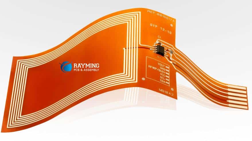
Flexible Laminates – Allow integration into curved surfaces and wearable applications.
There are many substrate material choices to optimize antenna performance versus cost for a given application. Some common options:
- PTFE Blends: Low loss, stable up to 100GHz
- Hydrocarbon Ceramics: Stable, low loss, moderate cost option
- Polyimide: Good flexibilty, moderate frequencies
- Low-loss FR4: A budget option, with frequency limitations
PCB Antenna vs Chip Antenna
Another antenna integration approach is using external packaged chip antennas. These contain a miniaturized antenna inside a small surface mount module. Where do chip antennas fit compared to PCB antennas?
Advantages of Chip Antennas:
- Extremely compact size
- Can be added to existing PCBs
- Mature, well-proven technology
- Good for portable/mobile applications
Advantages of PCB Antennas:
- Avoid external components
- Better efficiency and power handling
- Cost savings
- Improved ruggedness
- Higher gain options
- Greater design flexibility
In summary:
Chip antennas are quick and easy to implement but with performance limited by tiny size. PCB antennas provide superior performance through integration, but require upfront design effort.
PCB Antenna Future Trends
Like most electronics, antenna technology continues advancing rapidly. Here are some trends shaping the future of PCB antenna implementations:
- Higher Frequencies – Up to 100 GHz mmWave antennas using ceramic-filled PTFE substrates.
- 5G Integration – Massive MIMO antenna arrays with beamforming capabilities.
- Increased Digital Integration – Software defined antennas with tunable matching networks.
- Additive Manufacturing – Low volume antennas 3D printed on custom materials.
- Flexible Substrates – Antennas integrated on flex circuits and wearables.
- Multi-Functionality – PCBs incorporating wireless charging along with antennas.
- Low-Cost Materials – Innovative materials and ink-printed antennas on paper, textiles, etc.
- Autonomous Vehicles – High frequency, dynamic beam steering antennas for radar and V2X.
- IoT Growth – Continued antenna integration for compact, low cost wireless sensors.
The need for ubiquitous, high performance connectivity will continue driving PCB antenna implementations in nearly all types of electronic products.
Conclusion
Integrating antennas directly into printed circuit boards using standard PCB fabrication processes provides many benefits compared to traditional external antennas. Careful design of the shape and layout of the copper antenna elements allows PCB antennas to achieve excellent efficiency and gain. The trend towards wireless connectivity in almost all electronic products will expand the already widespread usage of PCB antennas across the telecom, auto, medical, consumer product, and industrial IoT segments.
Frequently Asked Questions
Q1: What are the main disadvantages of PCB antennas?
PCB antennas have a few disadvantages including design complexity, limited frequency range when using FR4, less flexibility than external antennas, and potential detuning from nearby components/objects.
Q2: How are PCB antennas tested during development?
Prototypes are tested using network analyzers to measure S-parameters. Radiation patterns, gain, and efficiency are measured in anechoic chambers. Environmental stress screening is also critical.
Q3: Can PCB antennas be used at frequencies over 6 GHz?
Yes, with careful design and using substrates with stable dielectric properties at those frequencies, such as PTFE blends or hydrocarbon ceramics. Performance above 20GHz requires specialized materials.
Q4: Can the same PCB contain both antenna elements and circuit traces?
Yes, in fact integrating antennas and circuitry is a key benefit. Care must be taken with layout to prevent interference between components and the antennas. Shielding and keepouts may be used.
Q5: Are there PCB antennas designed to work with multiple frequency bands?
Multiband antenna designs are common, such as combining cellular and WiFi bands into the same antenna structure through techniques like nested or intersecting elements resonant at different frequencies.


Leave a Reply