Introduction
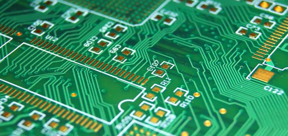
Silkscreen, also known as the solder mask, is a thin layer of epoxy or other material applied on top of a printed circuit board (PCB) to protect the copper traces from oxidation and prevent solder bridges from forming between closely spaced pads during assembly. The solder mask defines the solderable and non-solderable areas on the PCB and provides electrical and mechanical protection. It also serves an aesthetic purpose by allowing text, markings, and images to be printed on the board. This text and imagery printed on the solder mask is referred to as the silkscreen.
Silkscreen printing allows designers to easily identify components, indicate polarity, highlight connections, print reference designators, part numbers, board name/title, company logo, and other pertinent information directly on the PCB. This makes assembly and troubleshooting much easier. Let’s take a closer look at what silkscreen is, its functions, how it’s applied, and the silkscreen design process.
What is Silkscreen?
Silkscreen refers to the layer of ink or epoxy that is printed or etched onto the solder mask of a PCB. It usually contains text, lines, shapes, and images in various colors, traditionally white. The name comes from the silk fabric screens originally used to apply images onto PCBs.
The silkscreen legend serves many important functions:
- Identifies components – The reference designator, part number, logo, pin 1 marker, etc. help identify parts.
- Shows polarity – Symbols (+/-) indicate diode, capacitor, or IC orientation.
- Highlights connections – Dots, lines, and shapes show interconnections.
- Contains board information – Title, company, revision, date, copyright, etc.
- Improves aesthetics – Logos, lines, and colors make the PCB more appealing.
The silkscreen is like a stencil on top of the PCB, allowing selective marking without affecting the underlying copper. It provides a protective coating as well as a canvas for printed information.
Silkscreen Functions
Let’s look at some of the key functions of the silkscreen layer in more detail:
Component Identification
One of the primary purposes of silkscreen is to identify components on the PCB. Every part is given a designator such as R1, C3, U12, etc. which is printed on the silkscreen layer, usually in close proximity to the component. Manufacturers may also print the part number and sometimes the component value. This allows anyone working on the board to quickly identify any parts.
Reference designators and part info should be clearly visible, non-overlapping, and optimally oriented for easy reading. Fonts like vector fonts scale well.
Polarity Marking
Components like diodes, transistors, capacitors, and integrated circuits often need to be inserted in the correct orientation. The PCB silkscreen will use visual indicators like lines, shapes, and +/- signs near the component footprint to show the proper orientation.
For example, a triangle marks pin 1 of an IC. A solid or dashed line on a capacitor footprint shows its polarity. A diode has a solid line on the cathode side. These polarity markers prevent components from being accidentally inserted backwards.
Connection Highlighting
Silkscreen graphics are often used to highlight connections between components or different nets on the board. Dots, lines, arrows, and shapes can show how parts are interconnected. By tracing the silkscreen markings, you can follow a circuit path across the PCB.
For example, circles may be drawn around all nodes connected to ground. Lines can connect related pins of a multi-pin component. Arrows might show the direction of a data flow or control signal. This helps understand and debug the board’s circuits.
Board Information
Silkscreen text and images are used to label the board with identifying information like:
- Title – The board name and revision level, e.g. “Fire Alarm Panel Rev B”.
- Company name & logo – Who designed the board.
- Date – Release date or version info.
- Copyrights, patent info, other legal notices.
- Board notes – Warnings, instructions, descriptions.
- Version control – Revision numbers, designer initials.
- Unique IDs – Serial numbers, barcodes, macros.
This information helps identify the board and provides documentation for anyone working with it. The title and company branding also give the PCB a more professional look.
Improved Aesthetics
In addition to its functional purposes, the silkscreen layer allows designers to improve the appearance of the board. Silkscreen artwork can include:
- Company logos, symbols, and icons.
- Creative patterns, geometric shapes.
- Background colors, fills, gradients.
- Decorative elements and borders.
- Creative text fonts, sizes, and colors.
This allows a more appealing, finished PCB appearance. Silkscreen is often the most visible board layer, so can enhances or detracts from its look. A carefully designed silkscreen makes a positive visual impact.
How is Silkscreen Applied?
There are two main methods of applying the silkscreen layer to a printed circuit board:
Liquid Photoimageable Solder Mask
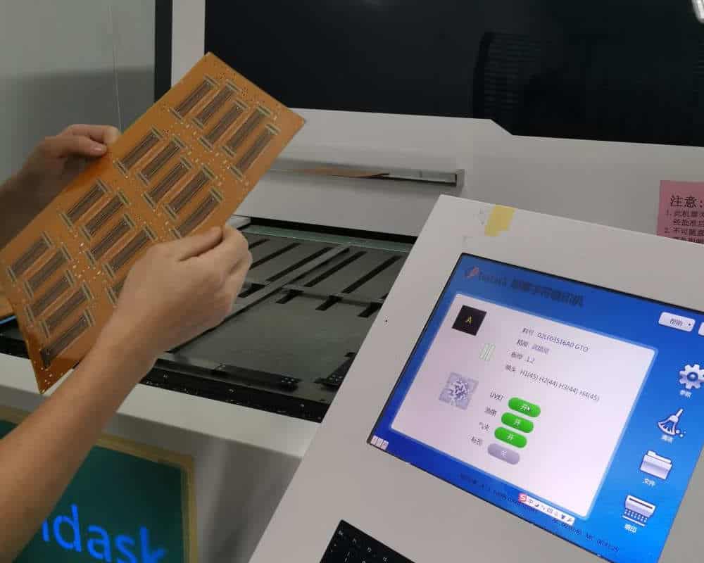
The most common method is to use a liquid solder mask material that is photoimageable. This allows the silkscreen layer to be patterned using photolithography, similar to the copper traces. Here are the steps:
- The PCB manufacturer applies a thin even coating of the solder mask material across the entire board surface. This forms the base layer.
- A photographic film image of the desired silkscreen artwork is placed over the PCB. The artwork may include both solid fill regions and clear areas.
- The board is exposed to UV light which hardens the solder mask in the artwork regions.
- The unexposed solder mask is washed away, leaving the desired silkscreen pattern.
- The board is oven cured to fully harden the remaining solder mask.
This process allows very accurate reproduction of silkscreen designs, including fine features. Various solder mask colors are available through different base materials.
Ink-Printed Silkscreen
Silkscreen printing originated from screens made of silk fabric. While less common today, ink printing is still used to apply silkscreens in some cases:
- A framed mesh screen with the silkscreen pattern is prepared.
- Ink is squeegeed through the open mesh onto the PCB surface.
- The board is oven or UV cured to harden the ink.
Ink printing allows thicker ink deposits and 3D texture effects. But fine features and registration accuracy are limited by the mesh resolution. This process is more cost effective for high volume PCBs using simple silkscreen graphics.
Silkscreen Design Process
Creating an effective silkscreen requires coordination between the PCB designer and the draftsperson developing the silkscreen artwork. Here is an overview of the typical silkscreen design process:
1. Planning
- Determine silkscreen content – Which info should be included on the board? Follow any company guidelines.
- Choose color palette – Standard is white, but additional colors may be used.
- Decide on graphics style – Company branding, icons, fonts, etc.
- Review manufacturing specs – Ensure artwork meets vendor requirements.
2. Drafting
- Create silkscreen text, images, logos, fills, etc. according to plan.
- Use CAD tools or graphic design software.
- Maintain required clearances from copper pads/traces.
- Include registration marks, tooling holes.
3. Review
- Check for errors, omissions, legibility.
- Have multiple team members review artwork.
- Confirm all info is conveyed clearly.
- Verify artwork meets specifications.
4. Submit to PCB Manufacturer
- Provide Gerber and drill files for all board layers.
- Include silkscreen file in manufacturer-compatible format.
- Specify solder mask type, silkscreen colors.
- Approve pre-production proofs to validate artwork.
5. Manufacturing
- Board house generates solder mask with integrated silkscreen layer.
- Uses photoimaging or printing process.
- Colors, accuracy, and quality may depend on vendors/costs.
- Validate production samples before full production run.
Careful planning and reviews help avoid problems in the finished boards. Good communication with the board manufacturer ensures the silkscreen is fabricated as designed.
Silkscreen Design Guidelines
Follow these guidelines when laying out the silkscreen for quality results:
- Legibility – Use an appropriate font size, line thickness, and high contrast. Avoid overlaps.
- Orientation – Place text so it is readable with the board orientation during assembly or use.
- Clearance – Keep silkscreen away from copper pads, traces, drill holes. Follow manufacturer guidelines.
- Consistency – Use the same identifiers, symbols, and conventions throughout.
- Simplicity – Cluttered silkscreens are confusing. Use only essential info.
- Accuracy – Avoid silkscreen info that may change, like dated info or revision numbers.
- Connections – Show connections with easy-to-follow lines, dots, arrows, etc.
- Polarization – Clearly indicate component orientation. Check footprint vs schematic symbols.
- Registration – Allow for alignment variations between layers. Provide safe clearances.
Following silkscreen design best practices results in professional-looking boards that are easy to assemble and troubleshoot.
Silkscreen Mistakes to Avoid
Here are some common silkscreen errors that should be avoided:
- Insufficient clearance – Silkscreen overlaps copper pads or traces risking bridges or obscuring connections.
- Wrong orientations – Component or text directions are unclear or misleading.
- Misalignments – Silkscreen markings don’t line up properly with their footprints.
- Unreadable text – Fonts too small, poor contrast, obscured by other features.
- Ambiguous references – Component identifiers are missing or confusing.
- Inaccurate connections – Lines, arrows, dots give wrong implications about circuit paths.
- Incorrect polarity – Component orientation indicators are wrong.
- Omitted information – Missing identifiers, part numbers, values, warnings.
Careful silkscreen design, reviews, and inspection at the board production stage minimizes such problems.
Advantages of Silkscreen
Some of the benefits provided by the PCB silkscreen layer include:
- Allows clear visual labeling of components, connections, and board details directly on the PCB surface.
- Eliminates need for separate assembly drawings, markings, and instructions.
- Makes assembly and servicing much easier with on-board component identification.
- Prevents incorrect insertion of polarized components with orientation indicators.
- Highlights circuit paths and interactions through connection markings.
- Provides protection for copper traces against environmental damage.
- Can improve aesthetics with company branding, logos, decorative elements.
- Allows certain unique board info, like serial numbers, to be customized on each PCB.
- Materials and processes used provide high durability and wear resistance.
For most boards, the advantages of incorporating a clearly designed silkscreen layer far outweigh the minimal additional production cost.
Disadvantages of Silkscreen
The silkscreen layer does have some disadvantages and limitations including:
- Additional cost, processing steps, and time to manufacture boards with silkscreen.
- More effort required for silkscreen design versus bare PCB layout.
- Extra steps needed in assembly if components must be installed prior to silkscreen application.
- Difficulty performing rework underneath hardened silkscreen layer. Modified boards may require full silkscreen stripping.
- Silkscreen graphics cannot be altered after board production. Any changes require a board respin.
- Low resolution and alignment tolerances can limit intricacy of silkscreen details.
- Colored silkscreens reduce contrast with darker components and markings.
- Excessive use of silkscreen can clutter board appearance.
Most of these disadvantages have minimal impact or can be mitigated through proper design. Overall, silkscreen improves manufacturability and usability of nearly all circuit boards.
Silkscreen vs Solder Mask
The terms “silkscreen” and “solder mask” are sometimes used interchangeably, but they refer to different board layers:
Silkscreen
- Graphics, text, and markings printed onto the solder mask layer.
- Provides visual information to aid assembly and use.
- Traditionally white, but other colors are also used.
Solder Mask
- The underlying epoxy or polymer layer covering the entire board.
- Leaves copper pads/traces exposed while protecting other traces.
- Usually green, but various colors are available.
- Electrically insulates copper from environment and adjacent traces.
So in summary:
- The solder mask is the protective colored background coating on the PCB.
- The silkscreen consists of the additional graphics, text, and markings selectively printed onto the solder mask.
Conclusion
The PCB silkscreen provides numerous benefits for manufacturing and use of printed circuit boards. This layer allows clear visual identification of components, orientations, board details, and functions directly on the surface of the board. Silkscreen improves aesthetics and conveys usage guidance without separate instructions. Implementation does require good communication between board layout and silkscreen artwork design. Following best practices for silkscreen design results in professional, user-friendly boards. The minimized additional cost is more than justified by the advantages.
Frequently Asked Questions (FAQ)
1. What are the typical silkscreen colors?
White silkscreen is the most common, providing good contrast on the green solder mask background. Other popular options include red, blue, yellow, black, and mirrored. Custom colors are also possible.
2. Does silkscreen go on top or bottom of PCB?
Silkscreen graphics normally go on both sides of the finished PCB for double-sided boards. For multilayer boards, silkscreen typically only goes on the outer surfaces.
3. How thick is the silkscreen layer?
Typical silkscreen thickness is around 0.0015 inches (0.038 mm). Thicker ink-printed layers up to 0.005 inches are also possible for increased durability or specialized applications.
4. What resolution and line width can silkscreen achieve?
Typical silkscreen line width ranges from 0.002 to 0.010 inches (0.05 to 0.25mm). Finer lines down to 0.001 inches are possible with some processes. Minimum line spacing is ~0.004 inches.
5. Does component height affect silkscreen application?
Yes, components taller than the silkscreen thickness will block application in their footprint area. Those components must be installed after silkscreening.


Leave a Reply