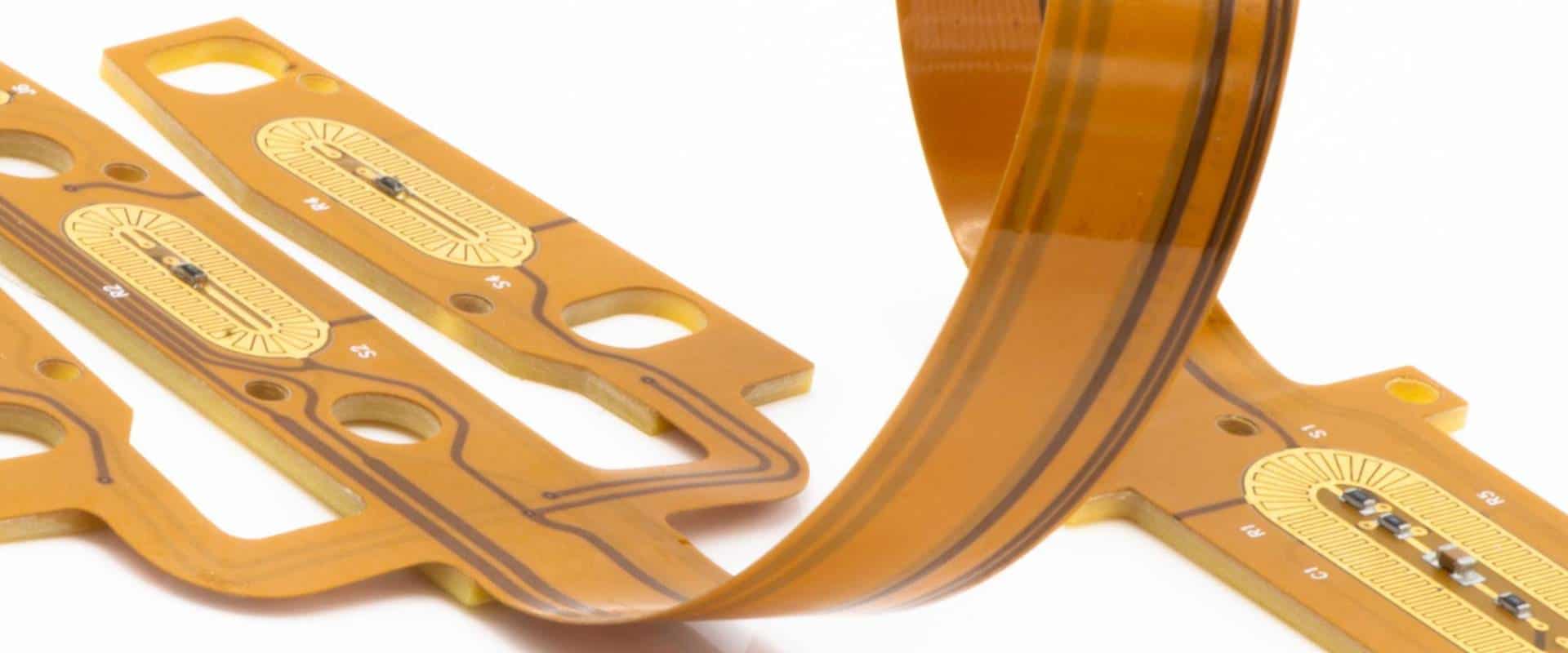
PCB (printed circuit board) prototyping is the process of designing, testing and manufacturing a preliminary version of a printed circuit board before full-scale production. Prototyping allows designers and engineers to evaluate the functionality, performance and manufacturability of a PCB design before committing to mass production.
Why Prototype Your PCB?
There are several key reasons to create a prototype PCB:
Verify the Design
Prototyping allows you to test your PCB design to uncover and fix any flaws or issues before manufacturing a large number of boards. It’s much cheaper to fix mistakes on a prototype rather thanscrap already manufactured boards. Prototyping lets you confirm:
- Functionality – Ensure your board operates and functions as intended.
- Errors – Find any errors or omissions in the design.
- Performance – Validate the signal integrity meets specifications.
- Manufacturability – Check that the board can actually be manufactured.
| Reason | Description |
|---|---|
| Verify Design | Test functionality, find errors, validate performance and manufacturability |
| Client Approval | Demonstrate design to client and get approval before full production run |
| Cost Savings | Cheaper to fix issues on a prototype rather than scrapping full production run boards |
| Faster Time-to-Market | Get working boards faster; test and refine design in parallel with other development activities |
Table: Key reasons to prototype PCB design
Client Approval
Prototypes let you demonstrate the design to stakeholders or clients and get their feedback and approval before investing in a full production run. This ensures the final boards meet their expectations.
Cost Savings
It’s significantly cheaper to fix issues with a design by tweaking a low-volume prototype rather than scrapping already manufactured boards in volume production. Re-spinning from an early prototype saves engineering time, reduces delays, and prevents wastage of fully-assembled boards.
Faster Time-to-Market
Prototyping enables working boards to be obtained quickly so hardware testing or software development can progress in parallel rather than sequentially. This accelerates overall development, allowing a product to launch faster. Issues can be addressed earlier too.
Types of Prototypes
There are a range of prototyping options and techniques available:
Breadboard Prototypes
A simple way to construct a circuit and test its operation without soldering is to use a breadboard. Components are inserted into the holes and secured by the spring-loaded clips inside. Wires make the connections between components. Breadboarding allows testing of circuit operation, enables tweaking component values and is useful early in development. However it does not test PCB layout considerations.
Stripboard Prototypes
Stripboard provides a grid of holes connected with copper strips on the bottom layer. By soldering wires and breaking traces between holes, custom circuit layouts can be achieved. Stripboard prototyping tests component choice, values and a near final circuit. But it still lacks the final form of a PCB.
Manhattan Style
A bare single or double-sided PCB has components glued or taped to the surface and point-to-point hand-wired together with insulated wire. This tests component choice and placement while allowing rework and probe access. But signal or power integrity issues can arise compared to a multilayer PCB with proper copper tracing.
Professional Prototypes
The most realistic prototypes use the same manufacturing techniques intended for production. These include:
- Rapid PCB Prototypes – Professional PCB prototype assemblers can manufacture boards in just 24-48 hours using automated equipment but lower volume processes. This quickly provides a realistic PCB to test.
- Limited Production Run – Producing a small batch of boards with the full capabilities and processes intended for high volume manufacturing checks not just design, but also manufacturability. Issues around automated assembly, soldering, handling or test can be uncovered.
For professional boards under low volume, costs range from $200-$500 for bare boards or $1000-$5000+ for assembled boards with components. Despite higher initial cost, finding issues here prevents vastly greater expense if discovered after commencing high volume production. Engineers can test with confidence the PCB matches final performance before progressing to mass production. Various online PCB prototype services exist to deliver boards exceptionally fast.
PCB Prototype vs Production
It’s important to understand how prototyping differs from full production:
| Factor | Prototype | Production |
|---|---|---|
| Volume | 1-10 boards | 100-10,000+ boards |
| Lead Time | 24-48 hours | Up to 4+ weeks |
| Capabilities | Hand assembly, lower technology process | Automated assembly, high-accuracy |
| Testing | Limited testing | Full specification testing |
| Cost | Higher cost per board, but fixed low total cost | Lower cost per board at high volumes |
| Purpose | Prove design viability | Manufacture product |
Table: Comparison of prototypes versus production PCB characteristics
Prototypes focus on design validation with fast turnaround as the priority even if the processes used differ from final manufacturing and cannot match production quality or economies of scale.
Whereas commissioned production PCBs place priority on high quality, reliability, repeatability and lowest cost-per board using high automation to maximize manufacturing volumes.
The PCB Prototype Process
The typical PCB prototyping process involves:
- Design schematic and PCB layout
- Generate Gerber files
- Order prototype boards
- Test prototype
- Repeat stages 1-4 until design is proven
1. Design Schematic and PCB Layout
The first step is creating the electronic schematic showing components and connectivity along with the PCB layout detailing physical placement and routing of copper tracks using CAD software tools like Altium Designer, Eagle, KiCad or OrCAD. This detailed design provides the blueprint for the PCB prototype.
Key questions to consider at design stage:
- Which components are required to construct the necessary circuit functions?
- How will components be arranged and interconnected on the PCB?
- Which is the optimal component placement for manufacturability, accessibility and serviceability?
- Can appropriate clearances be maintained around components considering manufacturability rules?
- Do copper tracks provide acceptable current rating and minimize noise based on your signal analysis?
- Are there any critical paths or RF performance factors requiring careful impedance control or isolation?
Simulating and pre-checking your design usingyour EDA tools eliminates many avoidable issues proceeding to prototype.
2. Generate Gerber Files
Completed PCB layouts are documented in a standard format called Gerber files that convey everything required to physically manufacture the bare boards.
The Gerber file set typically provides:
- Copper layers – detailing copper tracks and pads for components on each board layer
- Silkscreen overlay – legending to identify components, connections and text
- Solder mask layers – defining layer insulation areas
- Drill files – pinpointing hole sizes and locations
Cam files may also specify precise manufacturing details. Your PCB design software will handles exporting your completed layout into this standard machine-readable Gerber and drill format for PCB fabrication when you order prototypes.
3. Order Prototype Boards
Online PCB prototype services populate a web form asking key details like:
- Quantity of boards
- Layer count
- Minimum track width
- Material choice
- Finish
- Testing requirements
- Lead time
After uploading your Gerber files, the cost for bare or assembled boards is quoted for fabrication. Unit costs reduce as volumes increase from prototypes up to mid-volume batches while high volumes of 10,000+ leverage dedicated mass production lines.
For prototypes, hand assembly may be offered for faster delivery whereas production utilizes automated pick and place assembly. Lead times range from 24-48 hours for prototype quantities versus up to 4+ weeks for production volumes.
4. Test Prototype
Upon receiving your prototype PCB batch, they undergo testing. This typically includes:
- Visual checks – inspect soldering, assembly quality, physical defects
- Electrical validation – verify power consumption, outputs, functionality
- Debugging – identify and correct any functional or performance issues
- Environmental stress testing – check operation under extremes of temperature, vibration, humidity
- Compliance testing – confirm product meets safety or radio/EMC regulations
Testing prototyping is more limited than full production qualification but aims to reveal significant design or manufacturing faults.
5. Repeat Prototyping Process
For most projects, the design → prototype → test process iterates a number of revisions to incrementally improve, tweak and refine the design. Early prototypes focus more on core functionality, whereas later refinements concentrate on optimizing performance or manufacturability.
Each subsequent version increases confidence towards meeting the final production specification. Through successive prototypes, teething issues are ironed out prior to mass production.
When is Your PCB Design Ready for Production?
With each prototype build and test cycle completed, your design maturity increases towards readiness for volume manufacture.
Indications your PCB design is nearing production-ready status include:
- Circuit performs all intended functions correctly
- PCB layout achieves acceptable signal and power integrity
- No errors occur even with environmental or voltage stress testing
- Boards pass all regulatory standards testing first time
- Assembly and test yields from prototype builds meet targets
- Cost reductions no longer possible through design tweaks
- No major design changes anticipated
If these criteria sound feasible for your current design iteration, it may signify your design is primed for committed volume production. Nonetheless, it is smart to budget both time and cost contingency heading into initial production in case any residual issues sneak through requiring revision.
Who Needs PCB Prototypes?
Many players across the electronics development lifecycle leverage PCB prototyping to hone their designs, including:
Electronics Designers
To check circuit correctness, finalize component choice, tune values and prove PCB layouts are functional and manufacturable.
Hardware Product Engineers
To test form factor, manufacturability, reliability and performance meets specifications before release.
University Researchers
To experimentally validate novel concepts before peer review and publication.
Startups & Entrepreneurs
To demonstrate working prototypes to attract funding and capital investment before mass production.
For any new electronic hardware, access to rapid, low volume PCB prototype assembly enables real-world testing, risk reduction and design validation iterations not possible by simulation alone. This builds confidence prior to volume manufacture commitments.
FQA about PCB Prototyping
Some frequent questions about PCB prototyping include:
How Many PCB Prototype Revisions are Typical?
Most products span around 3-5 iterations from first prototype to final production design sign off, however simple or complex designs may converge faster or slower respectively:
- Version 1 – proves basic electrical operation but physical form factor usually deficient
- Version 2 – concentrates on optimizing layout, assembly and manufacturability
- Version 3 – achieves nearly final functionality and performance
- Version 4 – finalizes commercial design compliance and specifications
- Version 5 – marginal optimizations to reduce cost prior to mass production
Each subsequent prototype seeks to rectify issues from testing of the prior build.
Can I Make Changes to PCB Design Between Prototype Revisions?
Absolutely, prototypes exist to uncover improvements so your design can evolve. Allowable changes between revisions include:
- Component substitutions to alternate parts or values
- Shifting components to optimize signal paths
- Modifying or adding copper areas for heat relief
- Tweaking track width, isolation distances or pad sizes
- Replacing connectors or input locations
- Altering layer stacks to add or remove layers
By assessing initial prototypes, modifications for the next version target performance, reliability or safety problems observed in testing. Changes should stabilize as high volume production draws closer.
How Low Can PCB Prototype Volumes Go?
The lowest quantity is a single prototype board. Economies of scale apply so costs are higher for one-off boards versus batches. However prototype assemblers cater well for building a few to a few dozen boards. Typical minimum volumes are:
- 1-4 layer PCB – 1 board
- 6-8 layer PCB – 5-10 boards
Due to setup overheads, at least 5 units helps minimize cost per board for more advanced PCBs. Build volumes in the 1-25 unit range serve prototyping purposes well before escalating to pre-production volumes of 100+ units.
Is Hand Soldering Acceptable For Prototype PCBS?
Early prototypes may utilize hand assembly which is quick to implement and tolerates some design oversights. However deficiencies may only emerge during high speed automated production. Hand soldering suits initial concept verification however professionals recommend production-representative assembly for later prototypes. This reveals shortcomings around manufacturability while also testing reliability by subjecting prototypes to industry standard processes.
Can I Convert My Prototype PCB into High Volume Production?
If testing proves your design prototype sufficiently robust, the same Gerber design files and bill of materials utilized for prototyping should readily transfer for streamlined transition into volume PCB manufacture for commercial sale. Pre-checked designs port easily to mass production by simply increasing build quantities. Production will use dedicated manufacturing lines tailored for efficiency, precision and repeatability at high volumes not feasible during prototyping activities.
In summary, PCB prototyping provides in valuable design verification and risk reduction before large scale manufacture. Debugging flaws early saves considerable time and money compared with discovering issues after production. Engineering teams leverage prototyping to hone, improve and sign-off robust, reliable and functional designs ready for commercialization at volume. Through successive prototype build-test-repeat iterations, hardware products are refined to maximally balance performance, time-to-market and cost.


Leave a Reply