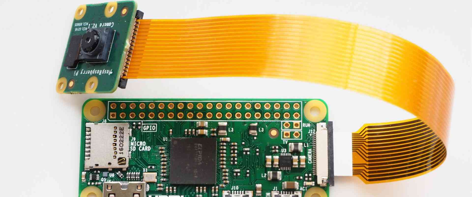
Printed circuit boards (PCBs) are integral components of most modern electronic devices. Ensuring PCBs function correctly is critical before deploying them into products. There are several testing methodologies that help validate PCB assembly and performance. This article explores the top PCB testing techniques.
What is PCB Testing?
PCB testing refers to methodologies and processes for validating the quality and functionality of printed circuit boards after manufacture. Testing confirms PCBs were correctly fabricated and assembled without errors or defects. It also verifies the board operates as intended within product design specifications.
Some key aspects tested during PCB validation include:
- Electrical connectivity
- Component placement
- Solder joint integrity
- Standoffs and proper fittings
- Absence of short circuits
- Appropriate insulation resistance
Common PCB testing methods covered in this guide include:
In-Circuit Testing
Flying Probe Testing
Boundary Scan Testing
Automated Optical Inspection
X-Ray InspectionICT Fixture Testing
Functional Testing
In-Circuit Testing
In-circuit testing (ICT) is one of the most widely adopted PCB testing methods used during manufacturing. ICT validates proper connections between components, checks for manufacturing defects, and verifies circuit board assembly.
How In-Circuit Testing Works
In-circuit testing utilizes fixtures containing probes that make contact with test points on a powered PCB. The tests stimulate inputs while monitoring outputs to check integrated circuits and discrete components function correctly.
Key aspects validated during ICT include:
- Presence of components
- Correct component values
- Proper insertion of parts
- Absence of solder defects
- Acceptable resistance tolerances
- No short circuits or opens
The fixture probes specific nets within the circuit to actively detect faults. This confirms all components were properly assembled and soldered during production.
ICT testers generate test programs based on computer aided design (CAD) data. This allows validating PCBs were assembled according to the bill of materials (BOM) and schematics.
In-Circuit Tester Configurations
There are several types of in-circuit testers and configurations including:
Parallel testers – Allow simultaneous testing of multiple test points
**Universal testers **- Support testing multiple board types
Dedicated testers – Optimized for testing a single PCB design
Manual testers – Require an operator to position boards
Automated testers – Robotic handlers manipulate boards
| Configuration | Description |
|---|---|
| Parallel | Multiple nodes tested concurrently for fast results |
| Universal | Flexible solution supports wide range of PCBs |
| Dedicated | Customized for specific board maximizing test coverage |
| Manual | Operator positions boards on fixture for each test |
| Automated | Robotic handlers manipulate boards allowing high volume |
Advantages and Disadvantages of ICT
Benefits of in-circuit testing:
- Identifies manufacturing faults
- Confirms components presence and solder integrity
- Validates proper assembly
- Extensive test coverage of nets
- Fast testing for high volumes
Downsides of ICT:
- Complex fixtures required
- Difficult testing dense boards
- Limited testing boards powered off
- Generates lots of test data to parse
In summary, ICT provides an efficient solution to validate overall PCB assembly and catch production issues. The tradeoff is fixtures can be costly and time-consuming to develop.
Real-World Examples of In-Circuit Test Systems
Teradyne UltraFLEX – High volume electronics test solution supports multiple generations of PCB designs. Handles boards up to 780mm x 560mm in size.
Seica Pilot V8 – Flexible flying probe style ICT tester does not require custom fixturing. Available in manual or automatic configurations.
Keysight Medalist i3070 – Universal in-circuit tester suitable for verifying complex medical and industrial electronics. Features multiple test heads with over 512 channels.
Flying Probe Testing
Flying probe testing is an alternative methodology to in-circuit testing without requiring custom test fixtures. Four or more movable arms with probes mechanically scan the PCB making temporary electrical connections. This dynamic contact allows checking nets across the board similar to ICT.
How Flying Probers Operate
Flying probe testers utilize cameras for optical recognition to identify components and capture board geometry. Proprietary software guides the arms to predefined test nodes. Resistance and voltage measurements validate circuit networks and nodes.
Steps of the flying probe testing process:
- Import CAD data
- Optically scan board features
- Translate data into test program
- Execute testing protocol
- Analyze results
- Generate test report
By eliminating physical test fixtures, flying prober systems accommodate multiple board types. Although test coverage may be less comprehensive than dedicated ICT solutions.
Types of Flying Probe Systems
There are several configurations of flying probers with different automation levels:
2 Probe Testers – Manually load individual boards which are secured to a transport fixture. Electric current limited to testing two nodes simultaneously.
4 Probe Testers – Most common style allowing greater net coverage by testing four cross points concurrently. Fixtures still required.
8 Probe Testers – High performance with eight independent arms for maximum simultaneous testing.
Automated Testers – Robotics used to handle and manipulate boards instead of fixtures. Enables seamless high volume testing.
| Type | Description |
|---|---|
| 2 Probe | Basic electric testing two nodes concurrently |
| 4 Probe | Most popular system testing four points simultaneously |
| 8 Probe | Advanced testing with eight independent probing arms |
| Automated | Robotics board handling for seamless high volume testing |
Advantages vs. Disadvantages
Benefits of flying probe testing:
- No custom fixturing required
- Tests multiple board types
- Validates SMT assembly and solder joints
- Identifies electrical opens and shorts
Downsides include:
- Slightly lower test coverage
- Slower testing than dedicated ICT
- Difficult probing ultra-fine pitch components
- Frequent tip cleaning and maintenance
Overall flying prober systems provide an adaptable solution to validate traceability and function without expensive custom fixtures.
Flying Probe Systems – Real World Examples
Takaya A8200 – High precision system handles boards up to 460mm x 360mm. Eight probes enable extensive simultaneous testing.
Seica Pilot 4D – Quad probe tester specializes in advanced PCBs like HDI boards. Also verifies conformal coating.
ATINOM HTF400-8 – Programmable automated handler and prober for testing eight points across large boards up to 610mm x 460mm.
Boundary Scan Testing
Boundary scan testing (BST) efficiently validates complex PCB assemblies and system-level interconnects. Also called IEEE 1149.1 standard test access port (JTAG), it leverages built-in infrastructure to diagnose faults.
Boundary Scan Basics
Boundary scan utilizes dedicated circuitry integrated into components on the PCB. Manufacturers implement JTAG circuitry to enable simplified testing of high pin count chips like FPGAs.
During testing, pin electronics get overridden allowing indirect I/O control. Serial test patterns injected to measure continuity and probe component logic.
As shown below, BST uses a four wire Test Access Port (TAP) to hijack pins:
| TAP Signal | Definition |
|---|---|
| TDI | Test Data In |
| TDO | Test Data Out |
| TMS | Test Mode Select |
| TCK | Test Clock |
This standardized boundary scan architecture eliminates physical test probes. BST directly accesses components through scan chains to validate interconnects on powered down boards.
Types of Boundary Scan Tests
Structural Tests – Validate board physical connections meeting continuity standards for traces and vias down to 0.1 ohm sensitivity. Checks all pins including balls under BGAs.
Cluster Tests – Probe component neighbor clusters to detect shorts without tracing entire networks. Focused validation of sections.
Interconnect Tests – Map connections by injecting signals and capturing bit data results to generate topology analysis correlated to CAD.
Boundary Scan Advantages
- Leverages existing embedded infrastructure
- Validates electrical connectivity
- Access components without physical probes
- Tests powered off boards
- Fine granularity fault identification
- Ideal for dense advanced packaging
Boundary Scan Limitations
- Requires compatible JTAG components
- Limited voltage or parametric testing
- Difficult high-speed signal analysis
- Software to generate tests can be complex
- Generating test coverage criteria is challenging
In summary, boundary scan testing delivers extensive fault coverage for board interconnects without physical test access. The tradeoff is compatible components required along with advanced software proficiency.
Boundary Scan Test Equipment
JTAG Technologies T3310 – High performance converter interfaces up to nine test adapters supporting over 10,000 test channels.
Goepel SPEA 4060 – Six TAP boundary scan controller for complex boards combining BST and ICT tests.
Keysight Medalist i3070 – Innovative universal in-circuit tester offering integrated boundary scan testing.
Automated Optical Inspection
Automated optical inspection (AOI) is an imaging based technique to visually examine PCB assemblies and components. Optical testing validates conformance, placement accuracy, component orientation as well as solder and adhesive defects.
Optical Inspection Overview
AOI surface scans populated boards using pattern recognition algorithms. Machine vision interprets images relative to electronic CAD drawings and centroid data. This optical metrology detects assembly problems like:
- Wrong or missing parts
- Skewed placements
- Insufficient clearances
- Poor solder fillets
- Scratches, dents or rips
AOI validation often complements X-ray imaging for verifying solder joints and internal features. Automated optical testing typically occurs after solder reflow before further integration.
2D vs 3D Optical Inspection
Two key optical inspection approaches include traditional 2D analysis augmented by advanced 3D techniques.
2D Inspection
- Assesses PCBs from a single camera angle
- Fast method to detect missing parts or polarity
- Unable to validate height or volume
3D Inspection
- Constructs three dimensional surface models from multiple views
- Provides volumetric dimensional analysis
- Quantifies coplanarity and protrusions
- Computationally intensive inspection
Utilizing both 2D optical recognition followed by 3D scanning maximizes test coverage and fault detection.
AOI System Examples
Koh Young KY8030-3 – High accuracy 3D AOI validates boards up to 510mm x 460mm. Six mega pixel cameras with four laser cross lines constructs detailed 3D images.
Omron VT-S1080 – Automated optical tester specializes in ultra-fine pitch inspection down to 01005 components. Handles range of board sizes.
Test Research TR7700QC – Quad camera simultaneous 2D and 3D analysis. OpenCV software controls robotic handler for automated optical testing.
X-Ray Inspection
X-ray imaging provides internal inspection to validate sub-surface features including solder joints, bonding wires, and component placement. It reveals hidden defects undetectable by optical examination.
Principles of X-Ray Testing
X-ray systems pass high energy radiation through a printed circuit board assembly. Denser objects like solder absorb more rays producing contrasting grayscale images used to analyze faults.
Typical aspects validated by x-ray inspection:
- Solder joint integrity
- Correct component insertion
- Absence of voids or cracks
- Proper lead formation
- Confirmation of hidden features
- Detection of foreign object debris
X-ray easily images components or connections concealed underneath ICs or behind PCB layers invisible to optical cameras.
2D and 3D X-Ray Configurations
X-ray inspection utilizes both two dimensional and 3D imaging:
2D X-Ray – Single planar views used for basic fault analysis like identifying missing pins underneath packages.
3D X-Ray – CT scanning constructs tomographic images by compiling multiple X-ray images during 360 degree rotational scan. Enables advanced volumetric dimensional inspection.
| Method | Description | Use Cases |
|---|---|---|
| 2D X-Ray | Single perspective images | Basic failure identification |
| 3D X-Ray | Volumetric CT scan models | Dimensional metrology, void analysis |
Utilizing both techniques provides comprehensive defect detection.
ICT Fixture Testing
ICT fixture validation provides an alternate method to confirm electrical connectivity and function after circuits are assembled into larger products. This late stage testing leverages fixtures emulating components of complete systems.
Fixture Based ICT Overview
After PCBs get integrated into bigger assemblies, directly probing nets becomes difficult. Fixture based tests emulate electrical connections allowing indirect in-circuit testing through a surrogate system.
Steps of the fixture testing methodology:
- Design fixture substituting for assembled product
- Connect analyzer to fixture access points
- Download baseline reference values
- Execute connectivity and functional validation tests
- Compare readings vs golden board criteria
- Document any discrepancies
This fixture based testing confirms subsystem PCBs were correctly integrated into larger products. It also allows testing repairs or validating replacement modules meet specifications.
ICT fixtures flexible to support evolving product generations unlike dedicated testers. Fixture solutions ideal for complex systems prohibitive for probing like automotive electronics.
Considerations of Fixture Based ICT
Advantages:
- Validate functionality and continuity of integrated PCBs
- Cost effective testing without custom testers
- Support multiple product variants
- Confirm repairs and replacement modules
Disadvantages:
- Significant upfront design effort
- Debugging faulty fixtures hampers testing
- Still requires some physical test access
- Indirect testing depends on fixture implementation
In summary, fixtures enable extended connectivity and performance validation testing otherwise impractical. The tradeoff is developing dependable fixtures represents a notable undertaking.
Functional Testing
Functional testing verifies boards operate correctly and withstand use cases replicating real-world conditions. This confirms PCBs perform intended functionality prior to deployment.
Purpose of Functional Testing
While structural defect testing evaluates board construction, functional validation focuses on use case operation including:
- Power up, power down sequencing
- Clock and timing analysis
- Simulating analog circuits and radio tuners
- Audio or video signal chains
- Integrating peripheral devices
Functional testers simulate inputs across multiple interfaces. This qualifies overall performance like throughput, accuracy, latency, synchronization, and reliability.
Steps of functional validation testing:
- Determine critical use cases and standards
- Build test model replicating interfaces
- Write test cases injecting inputs
- Continuously capture PCB outputs
- Analyze if performance meets product specs
- Repeat focused tests identifying defects
Thorough functional testing confirms the bare board operates correctly before getting deployed in field applications.
Functional Test Equipment Examples
Teradyne UltraFLEX – Features digital instrumentation integrating functional pattern processing including analog, digital, mixed signal, and protocol testing.
Chroma ATE 55200 – Test integration system stimulates multiple electronics interfaces synchronizing voltage, timing and loads validating functionality.
Goepel SPEA 3060 – Combines mixed signal ICT testing augmented by functional pattern generators confirming PCBs properly execute intended firmware logic.
FAQ – Frequently Asked Questions
Q: What are the benefits of in-circuit testing vs functional testing?
A: In-circuit testing efficiently validates manufacturing quality by detecting shorts, opens, missing components and solder defects. While functional testing confirms real-world use case performance meeting specifications. Utilizing both methodologies provides comprehensive PCB validation.
Q: Is flying probe testing or boundary scan testing better for advanced boards?
A: Flying prober systems flexibly accommodate multiple board types allowing simplified debugging of next-gen boards supporting rapid prototyping iterations. In contrast, boundary scan testing provides extremely detailed interconnect metrology mapping nets otherwise inaccessible – ideal for ultra-dense advanced boards.
Q: How accurate are AOI optical inspection vs X-ray detection?
A: Automated optical testing quickly scans for assembly issues like missing parts which X-ray can also identify. However X-ray inspection validates subsurface defects like solder joint integrity impossible to discern visually resulting in higher fault coverage.
Q: What approach is best to test repair modules?
A: Fixture based ICT testing allows validating replacement PCBs or subsystems meet specifications by emulating connectivity through surrogate networks. This efficiently confirms operation prior to directly swapping repaired components.
Q: Which PCB testing methodology has the highest throughput?
A: Parallel test in-circuit testers allow probing multiple test points simultaneously across large boards advancing quickly across nets. This produces fast results applicable for high volume manufacturing. High precision flying prober systems also achieve reasonable throughputs.


Leave a Reply