Introduction
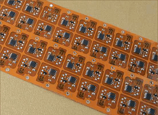
Printed circuit boards (PCBs) form the foundation of electronics, providing the mechanical structure and electrical interconnections for components. PCB fabrication, or manufacturing, is the complex multi-step process which transforms base materials into finished boards ready for component assembly and device integration.
Specialized companies focused exclusively on PCB fabrication are known as PCB manufacturers or PCB fabs. They’ve invested in advanced facilities and equipment to produce boards at scale across a wide range of specifications. This article provides an in-depth overview of PCB fabs – their capabilities, technologies, processes, and role supplying PCBs worldwide.
We’ll examine key aspects of professional PCB fabs including:
- Services offered and business models
- Manufacturing capabilities and limitations
- Step-by-step fabrication processes
- Quality control methods
- Comparison to small scale PCB production
Gaining insight into the workings of a PCB fab helps design engineers and procurement specialists source boards optimally for their products.
PCB Fab Services and Business Models
PCB fabricators offer a wide spectrum of services catering to customers across the full product lifecycle, from initial concept to volume production and beyond:
Prototype PCBs – Fast fabrication of 1-10 layer boards in small quantities for design testing and verification. Lead times range from 24 hours for basic boards to 7-10 days for complex prototypes.
Low Volume Production – Streamlined processes support builds of 10 to 1,000 boards, balancing speed, flexibility and affordable per unit pricing.
Medium Volume Production – Higher production runs from ~1,000 to ~10,000 boards benefit from economies of scale while maintaining quick turnaround.
High Volume Production – Extremely refined and automated manufacturing capable of producing over 10,000 boards per month at the lowest cost points.
Assembly Services – Populating fabricated bare PCBs with components using soldering processes. Offered standalone or bundled with board fabrication.
Quick Turn Special Services – Expedited fabrication, assembly, and shipping for urgent prototyping needs.
This range of services at varying lead times, volumes, and price points allows PCB fabs to meet the needs of diverse customers. From hobbyists to Fortune 500 OEMs, the right service model exists to deliver boards.
In addition to fabrication, most PCB fabs provide engineering support services:
- Design for Manufacturing (DFM) reviews and feedback during development
- Fabrication quoting based on board specs, layers, tolerances, and other factors
- Assembly quotes for stuffing boards with components after fabrication
- Testing and quality assurance services
These services combine with the core board fabrication capabilities to provide complete PCB production solutions.
PCB Fab Process Capabilities
Modern PCB fabs leverage extensive production infrastructure and technology expertise to fabricate even the most complex multilayer boards reliably at scale.
Some of the key fabrication capabilities include:
Layer Count – Mainstream production processes support up to 12 or 14 layers, with high density interconnect (HDI) techniques scaling up to 20 layers for advanced boards.
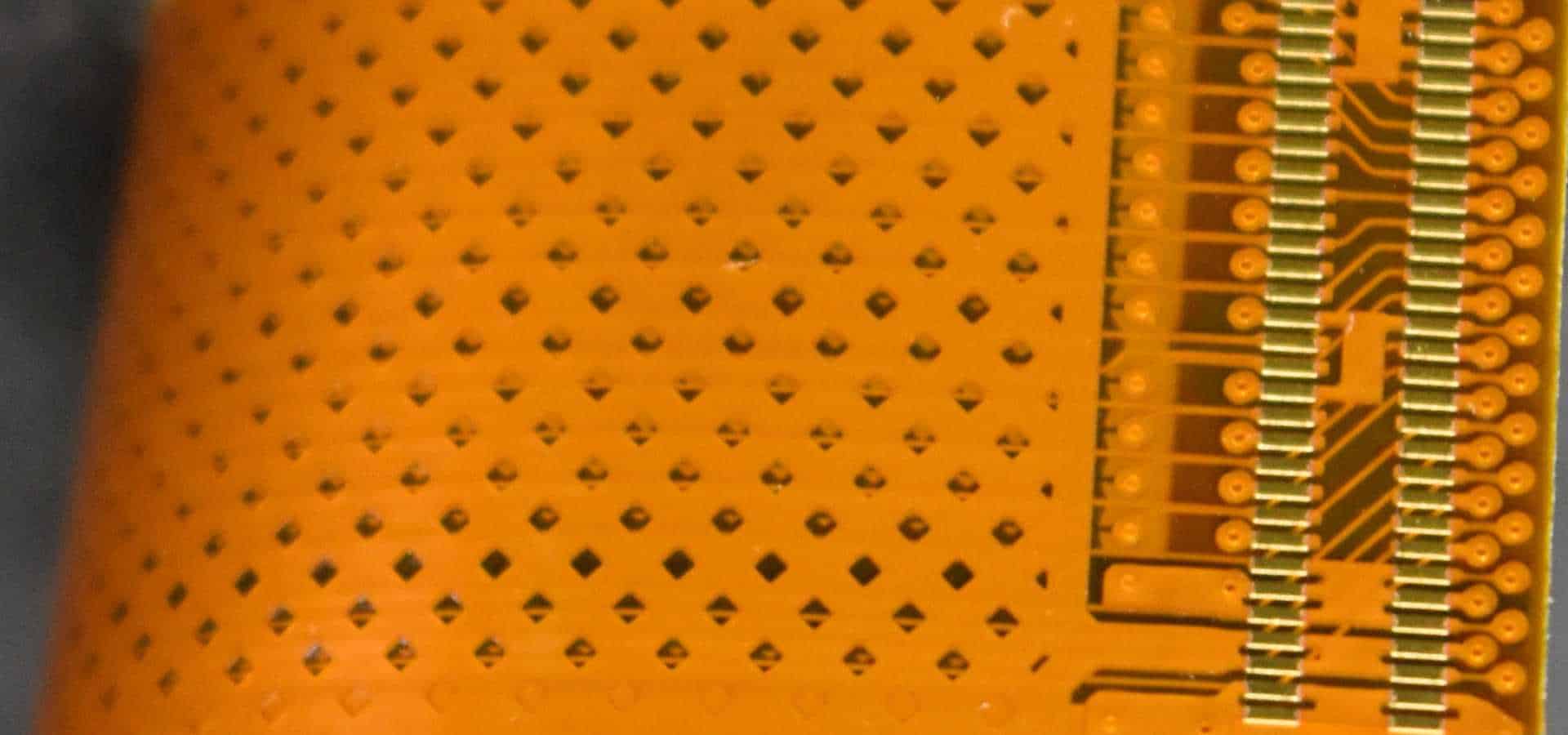
Board Thickness – Thicknesses reliably manufactured range from 0.4mm to around 5mm. Thinner flex PCBs down to 25um are also producible.
Board Size – Dimensions up to 600mm x 600mm can be produced, with smaller boards processed in panelized formats.
Line Width / Space – Ultra-fine line geometries down to 4mil (0.1mm) line and space are supported at mainstream fabs.
Via Structures – Various mechanically and laser drilled via types including through hole, blind, buried, and microvias enable vertical interconnects through a PCB stackup.
Surface Finishes – Multiple metallic and organic surface finishes are available from bare copper to immersion silver, ENIG, HASL, and more.
Materials – FR-4 continues dominating as the primary glass reinforced laminate material, with variants tailored for RF, thermal, flex, and high speed applications.
Standards – Compliance to IPC standards including IPC 6012 Class 2 and 3 are routinely met by professional PCB fabrication facilities.
These leading edge capabilities transform raw materials into the most sophisticated PCB technologies which drive modern electronic products.
However, every fabrication process has limits, and understanding PCB fabs’ constraints helps avoid designs that will be challenging or impossible to reliably manufacture. This may require compromises in areas like layer count, density, tolerances, and materials to balance performance with manufacturability.

Step-by-Step PCB Fabrication Process
PCB fabrication involves over a dozen major processes applied in sequence to transform raw base materials into finished boards.
The fabrication steps fall into three main stages:
1. Lamination
Creating the layered PCB structure from sheets of insulating material and copper foil.
- Material preparation – Cutting laminate and prepreg to size
- Layer stack lamination – Aligning and bonding all layers with heat and pressure
- Via formation – Drilling and plating holes to form vertical interconnects
2. Patterning
Selectively removing copper to leave only the desired traces and features.
- Imaging – Coating boards with photoresist and exposing in patterns
- Developing – Dissolving unset resist to expose copper regions for etching
- Etching – Removing exposed copper to form discrete traces and pads
- Stripping – Removing all remaining photoresist
- Outer layer imaging – Repeating exposure and etching on outer board surfaces
3. Plating and Finishing
Applying surface finishes, markings, and finalizing board geometry.
- Plating – Electroplating exposed copper pads/traces to increase thickness and solderability
- Coatings – Organic solder mask layers for insulation and markings
- Edge treatment – Beveling board edges
- Routing – Shaping boards by cutting into outlines
- Testing – Electrical testing, inspection, and quality control checks
This complex sequence of chemical, thermal, mechanical, and handling processes applied across dozens of boards maximizes productivity while maintaining quality.
Quality Control and Testing
Maintaining standards for quality and reliability requires rigorous process monitoring and sample testing during PCB fabrication:
- Visual inspection of innerlayers and outer layers at multiple steps checks for shorts, opens, contamination, and other defects
- Dimensional inspection confirms trace geometries, hole sizes, and critical distances are within tolerance
- Electrical testing using fixtures or flying probe testers verifies connectivity and isolates electrical defects
- Cross-sectioning and microscopy of plated holes and vias validates proper copper plating quality
- Microsectioning also measures actual dielectric thicknesses and trace geometries vs specifications
- Test coupons with daisy chains or test patterns quantify capabilities and yields for new processes
- First article inspection thoroughly validates all facets of new or changed designs
- Process control monitoring tracks key parameters like plating thickness, etchant concentration, lamination pressure, and more
This combination of monitoring, inspection, testing, analysis, and corrective action ensures consistency and high fabrication yields.
For mission-critical boards, steps like 100% automated optical AOI, intense functional testing, and X-ray inspection can further elevate quality levels.
PCB Mass Production vs Prototype Assembly
PCB fabs serve a crucial role in transforming board designs into high volume reality. However, for ultra-low volume prototyping it is also possible to fabricate boards in small quantities without a full professional fabrication facility:
Small Scale PCB Assembly
- Manual lamination of layers using household tools like clothes irons
- Chemical etching using simple acrylic or polypropylene containers
- Mechanical through hole drilling instead of advanced hole forming technology
- Manual paste masking and painting instead of panelized imaging
- Improvised metal electroplating setups
- Manual board shaping and tinning vs automated routing and plating
PCB Mass Production
- Automated layer lamination in heated hydraulic hot presses
- High accuracy photolithography patterning and etching
- CNC drilling, routing, and ablation machining
- Automated conveyorized plating lines
- Stringent process controls and quality monitoring
- Panelized processing for maximum throughput
- DFM rule checks and testing/inspection at every stage
- Statistical process control tracking all key performance indicators
The night and day differences in production scale, consistency, precision, and reliability motivate professional fabrication for most applications beyond initial prototyping experimentation.
Conclusion
PCB fabricators fill the crucial niche of transforming board designs into manufacturable and testable reality using leading edge fabrication techniques refined over decades. Their portfolio of services supports projects from early prototyping through to high volume product realization.
Understanding PCB fabs’ capabilities, limitations, processes, and quality control nuances builds effective partnerships between designers and their board suppliers. This empowers procuring boards which balance performance, lead time, and budget for a successful outcome.
So the next time you attend a product design review or place a new board order, remember the intricacies of the professional PCB fabs which support bringing your product vision to life.
Frequently Asked Questions
What are the main factors to evaluate when selecting a PCB fabrication vendor?
Key selection criteria include capabilities (features, tolerances, materials), quality level based on credentials and reviews, lead time and expedited service options, pricing and minimum order quantities, DFM review and engineering support, and production capacity scalability.
What fabrication technology limits board density and complexity?
The smallest achievable line width and space geometries restrict interconnect density. Mainstream PCB fabs can manufacture trace gaps down to around 4 mils (0.1mm) enabling up to 200 traces per inch. The finest processes support 2 mil features.
What are the most common quality issues encountered in PCB fabrication?
Typical defects include opens, shorts, insufficient etching, sputtering, pinholes in coatings, cracks, drill smearing, poor registration, plating voids, foreign object debris, and handling damage. Robust process controls and inspection aim to eliminate these errors.
How many drill and routing passes are required to fabricate a typical 6 layer FR-4 PCB?
Drilling proceeds from the center outwards as layers build up. A 6 layer board requires around 5 different drill passes. Routing proceeds from the outermost layers inward. Tab routing and full depanelization require 2 to 3 routing passes.
What are best practices PCB designers should adopt to ensure manufacturability?
Follow IPC design guidelines; maximize standardization of hole sizes, trace widths, and spacings; provide adequate clearances and annular rings; avoid trace geometries prone to etching or plating issues; utilize test and fill structures; communicate with your board shop.


Leave a Reply