Introduction
Printed circuit boards (PCBs) are an essential component of most modern electronic devices. A PCB serves as the physical foundation on which microchips, resistors, capacitors and other electronic components are mounted. The manufacturing process for PCBs involves many steps and techniques to transform raw materials into a functional board.
This comprehensive guide will walk through the entire PCB fabrication process, from design to final assembly. We’ll explore the key stages, including laminate materials selection, imaging, etching, cleaning, drilling, plating, silkscreen printing, electrical testing, population and more. Whether you’re an electronics engineer considering having PCBs made, or simply curious about how circuit boards are created, this article will provide an in-depth look at this fascinating industry.
Parts of a PCB
Before diving into the step-by-step manufacturing process, it’s helpful to understand the components that make up a completed PCB. The main elements are:
- Substrate – The base material that forms the structure of the PCB. Usually made of fiberglass epoxy laminate sheets known as FR-4.
- Copper layers – Thin sheets of copper foil that are laminated onto the substrate. The copper is etched away chemically to form the traces and pads.
- Solder mask – An epoxy based layer that is screen printed onto the PCB surface to insulate the copper traces.
- Silkscreen – Identifying markings printed onto the solder mask.
- Vias – Plated through-holes that connect traces between layers on multilayer PCBs.
- Pads – Exposed areas of copper to which electronic components are soldered.
- Traces – The copper pathways that electrically connect the pads.
Understanding these fundamental PCB elements will be helpful as we go through each step of the fabrication process.
PCB Design and Layout
The first phase in manufacturing printed circuit boards is designing the board itself. PCB layout involves building the interconnectivity of a circuit schematic into an actual physical design. This process is typically done with electronic design automation (EDA) software such as Altium, KiCad, or Eagle.
The designer will draw the trace layout, determine layer stackup, place component footprints, assign net names, add testpoints, and finalize all other aspects of the board artwork. This includes outlines for the location of cutouts, holes, silkscreen markings, and soldermask.
Some key considerations during PCB layout include:
- Component placement for optimal signal routing
- Trace widths based on current loads
- Impedance control for high speed signals
- Minimizing noise and crosstalk
- Thermal management of heat generating components
- Mechanical constraints for connectors, buttons, displays, etc
For complex boards, the designer may create a schematic first to map out the circuit logic, then convert it into a PCB layout. Simple boards can be laid out directly in the PCB design software. The final design files generated are usually Gerber and drill files that will be used for board fabrication.
Prototyping vs Production
There are two main types of PCB manufacturing:
Prototyping
- Small quantities
- Fast turnaround
- Lower costs
- Allows testing design before full production
Full Production
- Large quantities
- Longer lead times
- Higher costs
- Reliable manufacturing process
- Quality control testing
Prototyping is best suited during the design verification stage, while production runs are for finished boards that will be used in products. Many PCB manufacturers offer both prototyping and production services. The steps of the PCB fabrication process are essentially the same, but the specific techniques used may differ slightly.
We’ll be focusing this guide primarily on the full production PCB fabrication process, but will call out prototyping differences where applicable.
PCB Manufacturing Process Steps
Now that we’ve covered some essential background information, let’s walk through the step-by-step sequence of manufacturing a printed circuit board.
1. Sourcing Raw Materials
The fabrication process begins with sourcing all the required raw materials. This includes procuring the core substrate laminates, copper foil, soldermask epoxy, and other chemical solutions needed for etching, cleaning, plating, etc.
The main substrate material used today is FR-4 fiberglass epoxy. There are various grades of FR-4 that offer different properties in terms of thermal performance, strength, moisture absorption, and dielectric constants. Popular thicknesses range from 0.4mm to 3mm.
Copper foils come in different weights specified by ounces per square foot. Common weights are 1/8 oz, 1⁄4 oz, 1⁄2 oz, 1 oz, 2 oz, 3 oz, etc. Heavier copper is used for handling high power levels.
2. Inner Layer Production
The PCB fabrication process continues with preparation of the inner layers (for multilayer boards). First, both sides of the core substrate are laminated with photosensitive dry film. Next, the laminated substrate is put into an optical plotter where the circuit layout patterns are transferred from Gerber files onto the dry film using UV light exposure.
The exposed areas of dry film harden, while the unexposed areas remain soft. The board then goes through a chemical developing process to remove the soft, unexposed film, leaving behind a patterned layer of hardened photoresist.
The inner layer sheets now undergo an acid etching process which selectively removes the uncovered copper foil, while copper under the photoresist remains intact. Once etching is complete, the remaining dry film is stripped away leaving behind the designed inner layer circuitry.
3. Layer Alignment and Lamination
For multilayer PCBs, the individually etched inner layers are now precisely aligned and stacked in the designed sequence. Alignment accuracy at this stage is critical to ensure vias will interconnect between layers properly.
The core substrate and stacked laminates are placed in a lamination press and bonded together under high temperature and pressure. This fuses the layers into a single board. For boards with higher layer counts, the lamination process may be repeated to further build up the stack.
4. Drilling Holes
Using the drill files generated from the PCB layout software, the specific locations for holes are mechanically drilled into the laminated board. Holes are drilled for vias that interconnect layers, mounting holes, and openings for connectors or other components.
High speed CNC drill machines use small diameter twist drills spinning at high RPMs to achieve the necessary hole size accuracy and position precision. The drilling process also generates heat so cooling and swarf removal are important.
5. Hole Wall Preparation
After drilling, a combination of wet chemical processes are used to clean and prepare the hole walls for metalization. This can involve steps like sodium or potassium permanganate desmear to remove resin smear, plasma or chemical etching to roughen surfaces, and acid or plasma cleaning.
Proper hole wall prep removes debris, removes glass fibers, and improves adhesion to enable uniform coating of metal onto the hole walls.
6. Plating Copper
The next major PCB manufacturing process step is copper plating to make the through holes and vias conductive. This metallization process uses an electrolytic copper plating bath to deposit copper onto all the exposed surfaces.
First a very thin layer of copper is done through electroless plating which coats evenly across all areas. Then thicker copper is electroplated onto the base seed layer. Plating continues until the holes are fully filled.
After plating, a mechanical grinding or lapping process smooths down the surface and removes excess copper. This prepares the board for subsequent soldermask and silkscreen printing steps.
7. Soldermask Application
Soldermask is a key component of PCB fabrication. The soldermask epoxy layer coats the entire surface of the board except areas destined to be soldered. This serves both as insulation and to prevent bridging between traces.
Liquid photoimageable soldermask (LPI) is applied through a screen printing process. The board then undergoes UV light exposure with the soldermask artwork film followed by developing which chemically removes the unexposed areas. The final curing hardens the soldermask epoxy.
An alternative technique is laminated dry film soldermask in sheets that are applied and patterned through a similar lithographic process. Both methods produce the desired soldermask coverage.
8. Silkscreen Printing
Printing the silkscreen legend onto the soldermask is next in the sequence. The silkscreen layer adds informational text and markings like component designators, logos, board name, and other print.
The artwork is aligned on the PCB and the epoxy-based ink is screen printed directly onto the soldermask. Thermal curing then hardens the printed areas. Both liquid photoimageable and dry film soldermasks are compatible with silkscreen printing.
9. Surface Finishing
For many applications, PCB surface finishes are applied to enhance solderability while also protecting against surface oxidation. Common finishes include:
- Immersion Tin – Provides excellent solderability but prone to whiskering
- Immersion Silver – Excellent solderability and shelf life but tarnishes over time
- Electroless Nickel Immersion Gold (ENIG) – Widely used finish with good longevity
- Organic Solderability Preservatives (OSP) – Budget temporary coating
The specific finish chemistry, thickness, and application process depends on the requirements of the PCB. This finishing step is often performed by specialized vendors with selective plating equipment.
10. Electrical Testing
Before populated boards go to assembly, they typically undergo electrical testing. This quality control step verifies that the fabricated PCB matches the designed interconnectivity and functions as intended.
Testing methods include:
- Flying probe – Tests connectivity between pads
- Bed of nails – Makes contact through test points
- In-circuit test – Checks assembled board functionality
Issues like shorts, opens, impedance, leakage, continuity, and other faults can be detected to ensure defective boards are identified.
11. Assembly and Population
Once the blank PCBs have passed electrical testing, they are ready to be populated with components during assembly. This involves SMT pick and place machines mounting surface mount devices onto pads. Leaded components are inserted into drilled holes and soldered.
Additional steps in assembly include conformal coating for protection, heat sinks for cooling if needed, mechanical hardware, programming, etc. The fully assembled, populated boards are then put through a final suite of tests.
Prototyping vs Production PCB Manufacturing Process Comparison
While both prototype and production PCBs go through the same essential fabrication steps, there are some differences worth noting:
Prototyping
- Smaller batch sizes
- Flexible design changes
- Lower costs per board
- Faster manufacturing turnaround
- More manual processes
Full Scale Production
- High volume manufacturing
- Fixed, stable design
- Lower costs for large quantities
- Longer fabrication lead times
- Highly automated processes
- Additional testing and quality checks
So in summary, prototyping emphasizes fast iteration and design tweaks, while production focuses on reliability, repeatability, and volume output.
Factors That Influence PCB Fabrication Cost
There are a number of variables that determine the overall cost of manufacturing printed circuit boards. Understanding these key factors allows for smarter design decisions when balancing performance requirements and budgetary constraints. The main elements are:
Board Complexity
- Number of layers
- Component density
- Fine line/space traces
- High frequency designs
- Mixed-mode technologies
- Tolerancing and precision
Board Size
- Dimensions (length x width)
- Panel utilization percentage
Board Materials
- Substrate material type
- Copper weights
- Soldermask/silkscreen epoxy
- Use of finishes like ENIG, immersion silver etc
Testing
- Physical/visual inspection
- Automated optical inspection
- Flying probe
- In-circuit test
- Functional testing
Quantities
- Prototype vs production quantities
- Volume manufacturing pricing
Special Processes
- Tight impedance control needs
- Flex/rigid-flex boards
- HDI technology
- Via stitching at lamination
By optimizing these aspects, you can reduce PCB fabrication costs without compromising quality or functionality.
Key Takeaways
We’ve now explored PCB manufacturing from start to finish across these essential areas:
- The purpose and makeup of a printed circuit board
- PCB design considerations and layout
- Materials sourcing and inner layer fabrication
- Layer lamination and hole drilling
- Copper plating and soldermask application
- Silkscreen printing and surface finishing
- Electrical testing and final assembly
- Prototype vs production workflows
- Factors that determine fabrication pricing
This end-to-end overview covers the complete sequence of transforming raw materials into a populated, functional PCB assembly through precision fabrication techniques. Mastering the nuances of these processes will help guide both design choices and manufacturing decisions.
Frequently Asked Questions
What are the different types of PCBs?
The main types of PCBs are:
- Single sided – Copper traces on one side only
- Double sided – Copper on both top and bottom
- Multilayer – Sandwiched construction of multiple layers
- HDI – Boards with trace spacing and vias under 100 microns
- Rigid – Standard solid boards made of rigid FR4
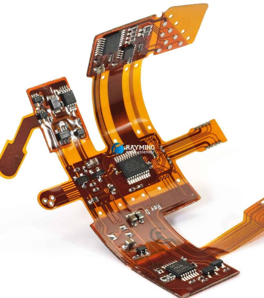
- Flex – Flexible circuits made of thin polyimide
- Rigid-flex – Combination construction of both
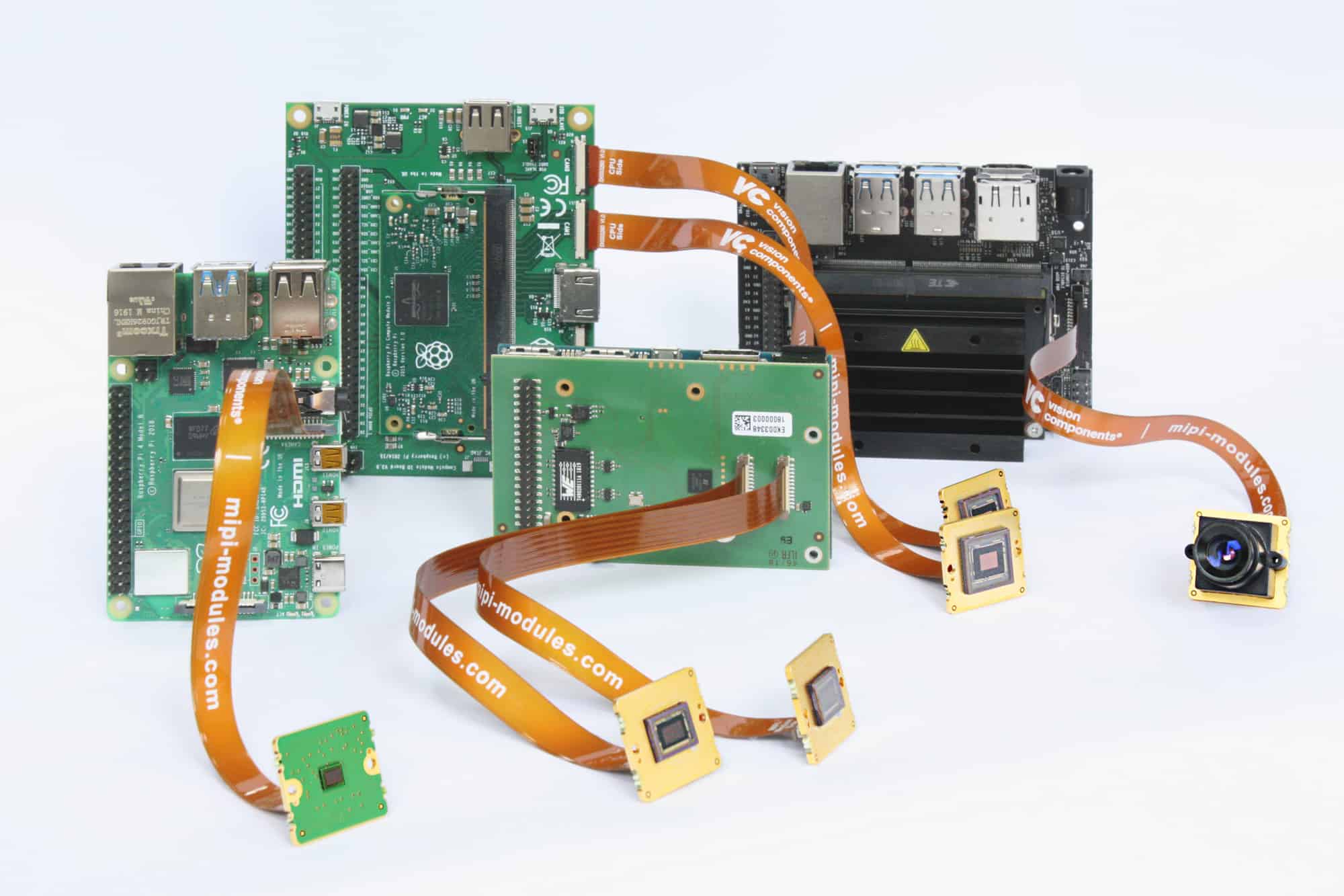
Can PCBs be manufactured at home?
It is possible to etch simple PCBs at home using household chemicals, but the process is generally low quality compared to professional fabrication. Home PCB manufacturing has very limited capabilities and is only suitable for hobbyist projects.
How long does PCB manufacturing take?
A typical production timeline once the design files are finalized is:
- Standard Spec Boards – 15-20 days
- Complex Boards – 20-30 days
Fast turnaround prototypes can be produced in as little as 24-48 hours.
What file formats do PCB manufacturers need?
The standard file formats are:
- Gerbers – For copper layers, soldermask, silkscreen etc
- Drill file – For hole locations
- BOM – Bill of materials listing all components
- Pick and place file – For SMT component locations
Can PCB manufacturers assemble boards as well?
Many PCB fabrication shops offer in-house assembly services to populate boards with components after manufacturing. Conformal coating and other post-processing steps may also be available.
This enables fully tested and assembled PCBs to be shipped to the customer. Some companies also integrate enclosure fabrication and other product fulfillment services.


Leave a Reply