Introduction
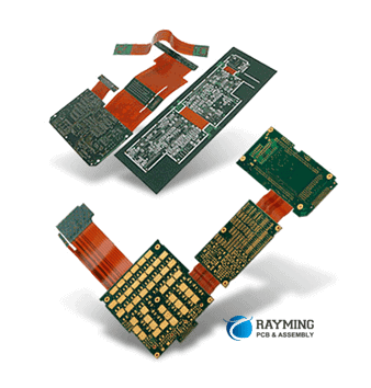
A rigid-flex printed circuit board (PCB) combines rigid and flexible substrate materials to create a circuit board that has both rigid sections and flexible folds or hinges. Rigid-flex PCBs allow three-dimensional configuration of electronic circuits and can improve reliability, space savings, and manufacturing automation.
Some common examples and applications of rigid-flex PCBs include:
- Cell phones – Folding rigid-flex PCBs connect components in the hinged sections of flip phones or allow flexing interconnections between components.
- Laptops – Interconnections between the base and lid sections can be made with rigid-flex material. Flexible sections allow opening and closing without wiring breakage.
- Medical devices – Flexible circuits can adapt to curving surfaces and motion in medical equipment housings.
- Automotive – Dashboard electronics and other automotive controls using rigid-flex PCBs can conform to spaces and tolerate vibrations.
- Wearable devices – The flexibility allows rigid-flex PCBs to accommodate natural contours and movements of the human body.
- Aerospace and military – Rigid-flex provides reliability in high vibration environments like spacecraft and aircraft.
This article provides an overview of rigid-flex PCB technology, construction methods, materials, design considerations, and examples of specific rigid-flex PCB implementations.
What is a Rigid-Flex PCB?
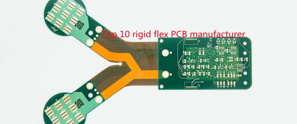
A rigid-flex PCB combines stiff, rigid circuit board sections with flexible interconnects on a single substrate. This allows adaptation to three-dimensional product enclosures, installation into areas not feasible with rigid boards, and dynamic flexing environments. Rigid sections provide structural stability for surface mount components and complex, multilayer circuitry. Flexible sections act as interconnection joints between the rigid segments, unfazed by repeated bending and twisting movements.
Rigid-flex PCBs bring several advantages compared to traditional rigid PCBs:
- Space savings: Folding rigid-flex PCBs require less space than interconnecting multiple rigid boards. The flex fold areas eliminate connectors between boards.
- Increased reliability: Flexible sections absorb vibrations, shocks, and motion instead of transmitting stresses to solder joints. This improves reliability and product life.
- Design flexibility: Rigid-flex allows adaptation to three-dimensional product enclosures that can’t fit typical planar circuit boards.
- Lower assembly costs: Automated component placement and soldering reduces manual labor costs compared to manually connecting multiple rigid boards.
Disadvantages include higher materials costs and more complex design and manufacturing processes.
Construction of Rigid-Flex PCBs
There are several design variations and materials used when constructing a rigid-flex PCB.
Layer Stackup
Like traditional PCBs, designers can specify different quantities of conductive copper layers separated by dielectric substrate layers. Typical rigid-flex layer counts include:
- Single-sided: Copper traces on one external layer only.
- Double-sided: Copper on both external layers.
- Multilayer: Two or more conductive inner layers for increased component density and routing options. Some rigid sections may have dozens of layers.
The layer stackup can transition between areas, such as a multilayer rigid section next to a single-sided flex area.
Dielectric Materials
The dielectric substrate provides electrical isolation between copper layers and mechanical structure. Common rigid-flex materials:
- Rigid sections: FR-4, polyimide, PTFE, ceramic-filled PTFE
- Flexible sections: Polyimide (Kapton), PTFE, PET
Polyimide films like Kapton provide the most flexibility but lack rigidity for populated sections. Rigid board materials like FR-4 have high flexural modulus for component support but are not truly flexible. Careful material selection balances the needs between rigid and flex areas.
Copper Thickness
Common copper foils in rigid-flex PCBs:
- 1 oz – Typical for outer layers and adequate for most traces
- 2 oz – Provides higher current capacity for power distribution
- 1/2 oz -Allows finer trace geometries, often used on inner layers
Thicker copper increases conductivity but also decreases flexibility. Flexible sections rarely exceed 2 oz copper.
Coverlayers
Additional polymer films like Kapton or acrylic can bond to the outer copper layers for protection, improved appearance, or bonding surfaces for conformal coatings. Coverlayers also help constrain the copper foil which improves flex resistance against cracking.
Bonded vs Mechanically Fastened
The rigid sections of a rigid-flex PCB can be fabricated separately and joined to the flex sections through:
- Bonding: Acrylic or epoxy adhesives permanently attach the flex to rigid sections. Bonded construction minimizes thickness.
- Mechanical fasteners: Screws or pins allow field assembly by connecting the rigid boards to threaded inserts in the flex areas. This allows servicing rigid sections separately. Fasteners increase thickness.
Stiffeners
Adding additional layers in the flexible area “stiffens” it to prevent unwanted bending. Common stiffening techniques:
- Copper stiffeners: Additional copper fills or thick traces reduce flexibility. Benefits include shielding and improved heat dissipation.
- Dielectric stiffeners: Added layers of rigid dielectric films reduce flexibility. Allows electrical isolation for any interior traces.
Rigid-Flex PCB Design Considerations
Designing a reliable rigid-flex PCB requires special considerations, including:
Layer Transitions
An abrupt transition between rigid and flex layers can lead to stresses and delamination. Methods to reduce layer transition stresses:
- Teardrops: Use an intermediate tapered section for a gradual transition.
- Fillets: Round the corners at layer transitions to reduce stress points.
- Slits: Cut lines partially into the rigid layers parallel to the edge to absorb bending forces.
Trace Routing
Traces crossing the bend line require:
- Teardrops at transitions: Smooths forces between rigid and flex sections.
- Narrower traces: Thinner copper traces withstand more bending without cracking.
- Plated half-etched traces: Reduces stresses by embedding the trace into the dielectric.
A minimum bend radius limits how tight the board can fold to avoid trace damage.
Component Placement
Strategies for smart component placement:
- Avoid flex area components: Minimizes stresses and weight on flexible sections.
- Surface mount devices: Easier to automate assembly than leaded components.
- Adhesives: Glue components near bend areas for more mechanical stability.
Vias
Plated through-hole vias electrically connect traces between layers. At layer transitions, they require:
- Fillets/teardrops: Rounded via transitions have less stress concentration.
- Adhesive collars: Bonds layers together and reduce flexing stresses on vias.
- Backfilled vias: Filling cut-outs with epoxy equalizes stiffness between layers.
Shielding
Electrical shielding helps prevent signal interference but ductile metal foil shields tend to crack at bends. Solutions include:
- Stiffeners: Added copper or dielectric layers allow thicker metal shields.
- Narrower folded shields: Minimizes cracking versus a single wide foil area.
Materials for Rigid-Flex PCBs
Selecting appropriate materials is critical for a functioning rigid-flex design.
Rigid Substrate Materials
The rigid sections of the PCB provide mechanical structure and stability for mounting components. Common materials used:
| Material | Description |
|---|---|
| FR-4 | Traditional glass-reinforced epoxy PCB material. Low cost but more prone to cracking on flexing versus polyimide. |
| BT (Bismaleimide Triazine) | Thermoset resin with glass fiber reinforcement. Withstands higher temperatures than FR-4. |
| PTFE (Polytetrafluoroethylene) | Known by the brand name Teflon. Maintains dielectric properties at microwave frequencies. |
| Ceramic-filled PTFE | Contains ceramic particle filler for increased dimensional stability but with less flexibility than unfilled PTFE. |
| Polyimide | Branded as Kapton when in film form. Withstands flexing without cracking. Used for rigid sections when some flexing is required. |
For most consumer and industrial electronics, FR-4 provides adequate performance at low cost. Applications requiring reliability at extreme temperatures, frequencies, or flexing conditions justify premium materials.
Flexible Substrate Materials
Common flexible dielectric films:
| Material | Description |
|---|---|
| Polyimide (Kapton) | High chemical resistance, 500°F temperature rating, resisting repeated flexing without cracking. High cost limits applications requiring larger area coverage. |
| PTFE | Withstands very high temperatures (260°C) without melting. Low dielectric loss at high frequencies. Expensive. |
| FEP | Fluorinated ethylene propylene. Modified form of PTFE with increased flexibility but reduced working temperature. |
| PET | Polyethylene terephthalate. Lower cost but limited chemical resistance and temperature range. |
| Polyurethane | Low cost flexible film with limited utility for typical PCB processing temperatures. |
For most rigid-flex PCBs, polyimide films like Kapton provide the best combination of physical and electrical performance properties in the flexible sections.
Rigid-Flex PCB Examples
Rigid-flex PCBs enable electronics designs not feasible with rigid boards alone. Here are some examples across different products.
Cell Phone Applications
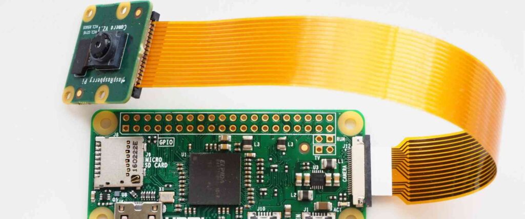
Early flip phones used ribbon cables or elastomeric connectors to link the folding sections. Rigid-flex PCBs simplified the phone construction and improved reliability.
Modern smartphone designs take advantage of folding rigid flex PCBs for:
- Interconnections from display to mainboard
- Buttons and connectors mounted directly on the flex section
- Flexing battery leads instead of wires
As smartphone form factors continue trending toward foldables, flexible PCBs will be increasingly critical.
Laptop and Tablet PCBs
Laptop designs must interconnect the base and lid sections while tolerating repeated opening/closing motions. Rigid flex PCBs simplify these connections:
Typical implementations include:
- Processor and power supply in base section
- Memory and wireless modules in lid section
- High-speed data links routed through flexible portion
- Flexible sections for screen and keyboard connectors
For tablets and convertible designs with removable keyboards, the keyboard ribbon cable can be replaced with a rigid-flex link.
Wearable Electronics
The flexibility of rigid-flex PCBs help conform wearables to the human body:
- Tight radii flex areas route traces around wrists and limbs
- Stretchable conductive inks withstand repeated expansions
- Rigid sections provide component mounting stability
- Can withstand washing and moisture for wearable textile electronics
Automotive Electronics
Vehicles contain many rigid-flex applications including:
- Instrument cluster and dashboard connections conform to spaces
- Engine control modules withstand engine vibration
- Flexible high-speed data bus replaces wiring harnesses
- Conform to curved surfaces like mirror adjustments
Medical Equipment
Medical devices often require compact, reliable circuitry to work in close patient proximity:
- Hearing aids fold into complex earbud shapes
- Endoscopes need traces wrapping around tubes
- Patient monitors and ECG leads conform to bodies
- Simplifies connections of replaceable modules
Rigid-Flex PCB Fabrication
Specialized processes manufacture the combination rigid and flexible materials in a PCB.
Laminating
Multiple material layers bond together under heat and pressure. The separate rigid and flex materials fuse into the composite result.
Etching
Photolithographic processes transfer the trace patterns onto the copper foil. Etchant chemicals remove unwanted copper, leaving the designed conductors.
Drilling
Laser, mechanical, and CNC drilling create the through-hole vias between layers. Flex areas require reduced drilling forces.
Plating
Metallization builds up conductive copper along the via holes and trace walls for connectivity between layers.
Solder mask
The solder mask layer insulates copper traces from unintended contacts and environmental exposure. LPI liquid photoimageable masks withstand flexing.
Test and inspection
Testing verifies electrical connectivity and performance under flexing. Automated optical inspection looks for defects.
Rigid-Flex PCB Design Software
Specialized rigid-flex PCB software tools integrate the front-end design, simulation, and manufacturing:
- Altium Designer: Unified design environment with rigid-flex features for trace transitions, layer stacks, and documentation.
- Mentor Xpedition: Systems-level PCB layout with rigid-flex modeling andanalysis.
- Cadence Allegro: PCB design with capabilities for modeling multilayer stacks with both rigid and flexible substrates.
- Siemens SolidEdge: MCAD and ECAD tools for designing enclosures and rigid-flex PCBs as an integrated system.
- ANSYS HFSS: Simulation of electrical performance, electromagnetic fields, parasitics and signal integrity in flexing conditions.
Most major PCB design packages now include functionality to handle mixed material electronics designs.
Conclusion
Rigid-flex PCBs provide an integrated solution for interconnecting electronics enclosures and components. The hybrid material technology combines the benefits of rigid board stability and flexible circuit adaptability. As electronic devices continue trending toward being more portable, wearable, and adaptable, rigid-flex PCBs become enabling technology to maintain connectivity and reliability. With specialized materials and layout adaptations, rigid-flex PCBs withstand mechanical stresses and create electronics package designs not feasible through rigid PCBs alone.
FAQ
What are the main advantages of rigid-flex PCBs?
The main benefits of rigid-flex PCBs include:
- Allows 3D configuration adapting to enclosures
- Withstands vibration, shock, and repeated flexing
- Saves space versus connecting multiple rigid boards
- Reduces assembly cost through automation
- Improves reliability by eliminating connectors
What are some typical applications of rigid-flex boards?
Common rigid-flex PCB applications:
- Cell phones – interconnections for folding and wearables
- Laptops – links between base and lid sections
- Medical equipment – curves and connections fitting the body
- Automotive – vibration resistance and conforming to spaces
- Aerospace – withstands acceleration and vibration conditions
What are suitable materials for flexible PCB substrates?
Common flexible dielectric films include:
- Polyimide (Kapton) – High performance but more expensive
- PTFE (Teflon) – Withstands high temp, chemically inert
- PET – Lower cost, lower maximum temperature
- Polyurethane – Very flexible but limited PCB capabilities
Polyimide is suitable for most high reliability flexible circuit needs.
How do designers ensure reliability on flexing areas?
Strategies for reliable rigid-flex PCB layouts include:
- Gradual transitions between rigid and flex sections
- Narrower traces routed perpendicular to bend line
- Teardrop vias to reduce potential cracking
- Kapton coverlay films to strengthen flex sections
- Avoiding components in flexing sections
How are multilayer rigid-flex PCBs fabricated?
Rigid-flex PCB fabrication involves:
- Laminating rigid and flex materials under pressure and heat
- Photolithography to produce trace patterns
- Precise laser and mechanical drilling
- Plating conductive traces on the via holes
- Bonding layers with adhesive films
- Testing electrical connections under dynamic flexing


Leave a Reply