Introduction to PCB Stack-Up
Printed Circuit Board (PCB) stack-up refers to the arrangement of layers in a PCB design. It is a crucial aspect of PCB design that determines the electrical performance, signal integrity, and manufacturability of the board. A well-designed PCB stack-up ensures that the signals are transmitted efficiently and accurately, while minimizing noise, crosstalk, and electromagnetic interference (EMI).
In this article, we will discuss the eight essential rules for designing a PCB stack-up that will help you create a reliable and high-performance PCB.
Rule 1: Determine the Number of Layers
The first step in designing a PCB stack-up is to determine the number of layers required for your design. The number of layers depends on the complexity of the circuit, the number of components, and the routing requirements.
| Number of Layers | Application |
|---|---|
| 1-2 | Simple designs with few components |
| 4 | Most common for medium complexity designs |
| 6-8 | Complex designs with high component density |
| 10+ | Very complex designs with high-speed signaling |
It is important to choose the right number of layers to ensure that the design is cost-effective and manufacturable.

Rule 2: Choose the Right Material
The choice of material for the PCB stack-up is critical for the performance and reliability of the board. The most commonly used materials for PCBs are:
- FR-4: A glass-reinforced epoxy laminate that is the most widely used material for PCBs.
- Rogers: A high-performance material used for high-frequency applications.
- Polyimide: A flexible material used for flex and Rigid-Flex PCBs.
The choice of material depends on the electrical and mechanical requirements of the design, such as the dielectric constant, dissipation factor, and thermal conductivity.

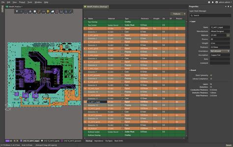
Rule 3: Define the Layer Stack-Up
Once you have determined the number of layers and the material, the next step is to define the layer stack-up. The layer stack-up specifies the arrangement of copper layers, dielectric layers, and plane layers in the PCB.
A typical 4-layer PCB stack-up is shown below:
| Layer | Description |
|---|---|
| Top | Signal layer |
| GND | Ground plane |
| PWR | Power plane |
| Bottom | Signal layer |
The arrangement of layers in the stack-up affects the impedance, crosstalk, and EMI performance of the board.

Rule 4: Control the Impedance
Impedance control is critical for high-speed designs to ensure signal integrity and minimize reflections. The impedance of a trace depends on the width of the trace, the thickness of the dielectric layer, and the dielectric constant of the material.
The target impedance for a trace can be calculated using the following formula:
Z0 = 87 / √(εr + 1.41) × ln(5.98 × h / (0.8 × w + t))
Where:
– Z0 is the characteristic impedance
– εr is the dielectric constant of the material
– h is the thickness of the dielectric layer
– w is the width of the trace
– t is the thickness of the trace
It is important to control the impedance of the traces to match the impedance of the source and load to minimize reflections and signal distortion.
Rule 5: Route the High-Speed Signals
High-speed signals require special consideration in PCB stack-up design to minimize crosstalk, EMI, and signal integrity issues. The following guidelines should be followed when routing high-speed signals:
- Route high-speed signals on the top or bottom layer of the board to minimize the length of the traces.
- Use a ground plane adjacent to the high-speed signal layer to provide a low-impedance return path and minimize crosstalk.
- Use differential pairs for high-speed signals to minimize EMI and improve signal integrity.
- Maintain a consistent spacing between the differential pairs to maintain the impedance of the traces.
Rule 6: Manage the Power Distribution
Power distribution is another critical aspect of PCB stack-up design. The power planes should be designed to provide a low-impedance path for the supply current and minimize the voltage drop across the board.
The following guidelines should be followed when designing the power distribution network:
- Use dedicated power planes for each supply voltage to minimize noise and crosstalk.
- Place the power planes close to the ground plane to minimize the inductance of the power distribution network.
- Use decoupling capacitors close to the power pins of the components to minimize the high-frequency noise on the power supply.
- Use a star topology for the power distribution network to minimize the voltage drop across the board.
Rule 7: Consider the Manufacturing Constraints
The PCB stack-up design should also consider the manufacturing constraints to ensure that the board is manufacturable and cost-effective. The following guidelines should be followed:
- Use standard layer thicknesses and materials to minimize the cost and lead time of the board.
- Avoid using buried or blind vias unless necessary to minimize the complexity and cost of the board.
- Use a minimum of 4 mil trace width and spacing to ensure manufacturability and reliability.
- Use a minimum of 6 mil drill size for through-hole vias to ensure manufacturability and reliability.
Rule 8: Verify the Design
The final step in PCB stack-up design is to verify the design using simulation tools and design rule checks (DRC). The following verifications should be performed:
- Signal integrity analysis to ensure that the signals are transmitted accurately and reliably.
- EMI analysis to ensure that the board meets the EMI regulatory requirements.
- Thermal analysis to ensure that the board can dissipate the heat generated by the components.
- DRC to ensure that the design meets the manufacturing constraints and design rules.
Frequently Asked Questions (FAQ)
Q1: What is the difference between a power plane and a ground plane?
A: A power plane is a copper layer that is used to distribute power to the components on the board, while a ground plane is a copper layer that is used to provide a low-impedance return path for the signals.
Q2: What is the purpose of using differential pairs in high-speed designs?
A: Differential pairs are used in high-speed designs to minimize EMI and improve signal integrity. Differential signaling uses two traces to transmit a signal, with one trace carrying the positive signal and the other carrying the negative signal. This cancels out the common-mode noise and minimizes the EMI radiation from the board.
Q3: What is the difference between a blind via and a buried via?
A: A blind via is a via that connects an outer layer to an inner layer, but does not go through the entire board. A buried via is a via that connects two inner layers, but does not connect to the outer layers.
Q4: What is the purpose of using decoupling capacitors in power distribution?
A: Decoupling capacitors are used to minimize the high-frequency noise on the power supply and provide a local source of charge for the components. They are placed close to the power pins of the components to minimize the inductance of the power distribution network.
Q5: What is the purpose of using a star topology for power distribution?
A: A star topology is used for power distribution to minimize the voltage drop across the board. In a star topology, the power is distributed from a central point to the components, minimizing the resistance and inductance of the power distribution network.
Conclusion
Designing a PCB stack-up is a critical aspect of PCB design that requires careful consideration of the electrical, mechanical, and manufacturing constraints. By following the eight rules discussed in this article, you can create a reliable and high-performance PCB that meets your design requirements.
Remember to choose the right number of layers and materials, define the layer stack-up, control the impedance, route the high-speed signals, manage the power distribution, consider the manufacturing constraints, and verify the design using simulation tools and DRC.
By following these rules and guidelines, you can create a PCB stack-up that ensures signal integrity, minimizes noise and EMI, and is manufacturable and cost-effective.


Leave a Reply