What is an AOI Test?
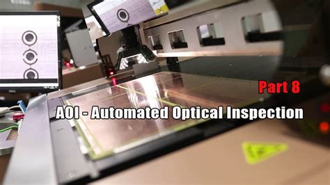
An Automated Optical Inspection (AOI) test is a automated visual inspection process used to detect defects or anomalies in printed circuit board (PCB) assemblies. AOI tests use high-resolution cameras and image processing software to quickly scan and analyze PCBs for missing components, incorrect component placement, solder defects, and other quality issues.
AOI testing is a critical step in PCB manufacturing to ensure the reliability and functionality of the final product. It allows manufacturers to identify and correct defects early in the production process, saving time and costs compared to catching defects later or after the product is shipped.
Key Features of AOI Tests
| Feature | Description |
|---|---|
| High-speed inspection | AOI machines can scan PCBs at speeds up to 1.5 m/s, allowing for fast throughput |
| High-resolution imaging | Cameras with resolutions up to 25 microns can detect even the smallest defects |
| Multiple viewing angles | AOI machines often have multiple cameras positioned at different angles to thoroughly inspect all sides of components |
| Defect classification | Advanced algorithms can classify defects by type (e.g. missing component, solder bridge) for easier review and correction |
| Integration with manufacturing line | AOI machines can be integrated inline with pick-and-place machines, reflow ovens, and other equipment for seamless inspection |
How Does an AOI Test Work?
The AOI testing process typically involves the following steps:
-
PCB Loading: The PCB assembly is loaded into the AOI machine, either manually or automatically using a conveyor system.
-
Image Capture: High-resolution cameras capture images of the PCB from multiple angles. The number of cameras and viewing angles varies depending on the complexity of the PCB and the level of inspection required.
-
Image Analysis: The captured images are processed by computer algorithms that compare them to a reference image of a known good board. The software looks for any deviations or anomalies, such as missing components, incorrect component placement, solder defects, etc.
-
Defect Classification: If any defects are detected, the software classifies them by type and severity. This information is used to generate a report for the operator to review.
-
Operator Review: The operator reviews the defects flagged by the AOI machine and decides whether to accept or reject the board. Some AOI systems allow the operator to make minor repairs or adjustments to the board during this step.
-
Data Collection: The AOI machine collects data on the number and types of defects found, which can be used for process improvement and traceability.
AOI Test Process Flow
graph LR
A[PCB Loading] --> B[Image Capture] --> C[Image Analysis] --> D[Defect Classification] --> E[Operator Review] --> F[Data Collection]

Types of Defects Detected by AOI Tests
AOI tests can detect a wide range of defects on PCB assemblies, including:
- Missing components: Components that are missing from the board entirely.
- Misaligned components: Components that are not placed accurately on the pads.
- Incorrect components: Components that are the wrong type or value for the designated location.
- Solder defects: Insufficient, excessive, or bridged solder connections.
- Polarity defects: Components that are placed with the wrong polarity.
- Damaged components: Components that are physically damaged or have bent leads.
Common PCB Defects
| Defect Type | Example Image |
|---|---|
| Missing component | |
| Solder bridge | |
| Incorrect component | |
| Insufficient solder |

Benefits of AOI Testing
Implementing AOI testing in PCB manufacturing offers several key benefits:
-
Early Defect Detection: AOI tests allow manufacturers to catch defects early in the production process, before the board moves on to more expensive testing or rework steps. This helps to reduce scrap and rework costs.
-
Improved Quality: By detecting and correcting defects that might be missed by manual inspection, AOI testing helps to improve the overall quality and reliability of the final product.
-
Increased Throughput: AOI machines can inspect boards much faster than human operators, allowing for higher production throughput and shorter lead times.
-
Objective and Repeatable: AOI tests provide objective and repeatable results, eliminating the variability and subjectivity of human inspection.
-
Traceability: AOI machines collect data on the number and types of defects found, which can be used for process improvement and traceability. This data can help manufacturers identify trends and root causes of defects.

Limitations of AOI Testing
While AOI testing offers many benefits, it also has some limitations:
-
Limited Depth Perception: AOI cameras can only see the surface of the board, so they may miss defects that are hidden under components or within the board itself. Additional testing methods, such as X-ray inspection, may be needed for these types of defects.
-
False Positives and False Negatives: AOI algorithms can sometimes flag defects that are not actually present (false positives) or miss defects that are present (false negatives). Operator review and fine-tuning of the algorithms can help to reduce these errors.
-
Component Variations: AOI systems may struggle with inspecting components that have a high degree of variation, such as odd-shaped or reflective components. Special lighting or image processing techniques may be needed for these cases.
-
Programming Complexity: Setting up an AOI machine to inspect a new PCB design can be a complex and time-consuming process, requiring skilled programmers to create the reference images and inspection algorithms.
AOI vs. Other Inspection Methods
AOI testing is just one of several methods used for PCB inspection. Other common methods include:
-
Manual Visual Inspection (MVI): Human operators visually inspect the board using magnification and lighting. MVI is slower and more subjective than AOI but can catch some defects that AOI might miss.
-
In-Circuit Testing (ICT): Electrical probes are used to test the functionality of individual components and circuits on the board. ICT can detect defects that are not visible to AOI, but it requires physical contact with the board and custom test fixtures.
-
Flying Probe Testing: Similar to ICT, but uses moving probes instead of a fixed test fixture. Flying probe testing is more flexible than ICT but slower.
-
X-Ray Inspection: X-ray imaging is used to see through the board and inspect hidden solder joints and internal components. X-ray inspection can detect defects that are not visible to AOI but requires more expensive equipment and safety precautions.
Comparison of PCB Inspection Methods
| Method | Pros | Cons |
|---|---|---|
| AOI | Fast, objective, non-contact | Limited depth perception, false positives/negatives |
| MVI | Can catch some defects missed by AOI | Slow, subjective, labor-intensive |
| ICT | Tests functionality, detects hidden defects | Requires custom fixtures, physical contact |
| Flying Probe | Flexible, tests functionality | Slower than ICT |
| X-Ray | Detects hidden defects | Expensive, requires safety precautions |
Implementing AOI in PCB Manufacturing
To successfully implement AOI testing in a PCB manufacturing process, consider the following steps:
-
Define Inspection Requirements: Determine which defects are critical to detect and what level of inspection coverage is needed for each PCB design.
-
Select an AOI System: Choose an AOI machine that meets the inspection requirements and integrates well with the existing manufacturing line. Consider factors such as camera resolution, speed, programming ease, and cost.
-
Develop Inspection Programs: Create reference images and inspection algorithms for each PCB design. This may require skilled programmers and close collaboration with the design team.
-
Train Operators: Provide training for operators on how to load boards, review defects, and make repairs as needed. Develop clear procedures for handling defects and escalating issues.
-
Monitor and Optimize: Regularly monitor the performance of the AOI system and analyze defect data for trends. Use this information to optimize the inspection programs and identify opportunities for process improvement.
FAQ
Q: How much does an AOI machine cost?
A: The cost of an AOI machine can vary widely depending on the features and capabilities. Entry-level machines may cost around $50,000, while high-end machines with advanced features can cost $500,000 or more. In addition to the initial equipment cost, there are also ongoing costs for maintenance, programming, and operator training.
Q: Can AOI replace manual visual inspection entirely?
A: While AOI can greatly reduce the need for manual visual inspection, it is often used in combination with other inspection methods for best results. AOI can quickly catch most surface-level defects, while manual inspection can provide a final check for any defects missed by AOI. The right balance of inspection methods depends on the specific product and quality requirements.
Q: How long does it take to program an AOI machine for a new PCB design?
A: The time required to program an AOI machine for a new PCB design can vary depending on the complexity of the board and the skill of the programmer. Simple boards may only take a few hours to program, while complex boards with many components and fine-pitch devices can take several days or even weeks. Ongoing maintenance and updates to the inspection program are also required as the PCB design evolves.
Q: Can AOI detect counterfeit components?
A: AOI can detect some signs of counterfeit components, such as incorrect markings or dimensions. However, more advanced methods such as X-ray inspection or electrical testing may be needed to definitively identify counterfeit parts. It’s important to also have strong supply chain controls and traceability to prevent counterfeit components from entering the production process.
Q: What is the difference between 2D and 3D AOI?
A: 2D AOI uses standard 2D image processing techniques to inspect the surface of the PCB, while 3D AOI uses techniques such as structured light or laser scanning to create a 3D model of the board. 3D AOI can provide more detailed information about component height and coplanarity but requires more advanced hardware and software. The choice between 2D and 3D AOI depends on the specific inspection requirements and budget.


Leave a Reply