Step 1: Define Microwave PCB Requirements
Before starting the design process, clearly define the requirements for your microwave PCB. Consider factors such as:
- Frequency range
- Signal power levels
- Impedance matching
- Component placement
- Board size and shape
- Environmental conditions
Having a well-defined set of requirements will help streamline the design process and ensure that your microwave PCB meets the desired specifications.
Step 2: Choose the Right Substrate Material
Selecting the appropriate substrate material is crucial for microwave PCB design. The substrate material affects the electrical properties, thermal stability, and mechanical strength of the PCB. Common substrate materials for microwave PCBs include:
- Rogers RO4000 series
- Taconic RF-35
- Isola I-Tera MT40
- PTFE (Polytetrafluoroethylene)
Consider the dielectric constant, dissipation factor, and thermal expansion coefficient of the substrate material to ensure compatibility with your design requirements.

Step 3: Determine the Layer Stack-up
The layer stack-up of a microwave PCB plays a vital role in signal integrity and impedance control. A typical microwave PCB stack-up consists of:
- Signal layers
- Ground planes
- Power planes
- Dielectric layers
Carefully plan the layer stack-up to minimize crosstalk, reduce electromagnetic interference (EMI), and maintain consistent impedance throughout the PCB.

Step 4: Calculate Trace Widths and Impedances
Calculating the appropriate trace widths and impedances is essential for maintaining signal integrity in microwave PCBs. Use impedance calculators or simulation tools to determine the optimal trace widths based on the substrate material, layer stack-up, and desired characteristic impedance (usually 50 ohms).
Consider the following factors when calculating trace widths:
- Substrate dielectric constant
- Substrate thickness
- Copper thickness
- Trace spacing

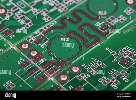
Step 5: Design Microwave Transmission Lines
Microwave transmission lines are critical components in microwave PCB design. They are responsible for guiding high-frequency signals with minimal loss and distortion. Common types of microwave transmission lines include:
- Microstrip
- Stripline
- Coplanar waveguide (CPW)
- Grounded coplanar waveguide (GCPW)
Select the appropriate transmission line type based on your design requirements, frequency range, and substrate material. Use simulation tools to optimize the transmission line dimensions and ensure proper impedance matching.
Step 6: Implement Impedance Matching Techniques
Impedance matching is crucial for minimizing signal reflections and ensuring maximum power transfer in microwave PCBs. Implement impedance matching techniques such as:
- Quarter-wave transformers
- Tapered lines
- Stub matching networks
- Lumped element matching networks
Use simulation tools to design and optimize impedance matching networks for your specific microwave PCB layout.
Step 7: Minimize Discontinuities and Parasitics
Discontinuities and parasitics can introduce unwanted signal distortions and reflections in microwave PCBs. To minimize their impact:
- Avoid sharp bends and corners in transmission lines
- Use smooth transitions between different transmission line types
- Minimize via usage and optimize via geometry
- Keep trace lengths as short as possible
- Use ground stitching vias to maintain a consistent ground reference
Step 8: Implement Proper Grounding Techniques
Proper grounding is essential for maintaining signal integrity and reducing EMI in microwave PCBs. Follow these grounding techniques:
- Use a solid ground plane beneath microwave components and transmission lines
- Implement ground stitching vias to connect ground planes on different layers
- Avoid split ground planes, as they can introduce unwanted resonances
- Use multiple ground vias for component grounding
Step 9: Optimize Component Placement
Component placement is critical for microwave PCB performance. Follow these guidelines:
- Place components close to their associated transmission lines to minimize parasitic effects
- Avoid placing components too close to board edges to reduce coupling and radiation
- Maintain symmetry in component placement to minimize unbalanced signal paths
- Consider the component’s footprint and orientation for optimal signal routing
Step 10: Route High-Frequency Signals Carefully
Routing high-frequency signals in microwave PCBs requires special considerations:
- Route high-frequency signals on the top layer whenever possible
- Avoid crossing signal traces to minimize crosstalk
- Maintain consistent trace widths and spacing to maintain impedance
- Use smooth curves instead of sharp bends to minimize discontinuities
- Avoid routing high-frequency signals near board edges to reduce radiation
Step 11: Implement Shielding Techniques
Shielding is important for reducing EMI and crosstalk in microwave PCBs. Implement shielding techniques such as:
- Using shielding enclosures for sensitive components
- Implementing guard traces around high-frequency signals
- Using shielding vias to create a Faraday cage around sensitive areas
- Applying conductive coatings or adhesives to the PCB surface
Step 12: Consider Thermal Management
Thermal management is crucial for microwave PCBs due to the high power dissipation of microwave components. Consider the following thermal management techniques:
- Use a thermally conductive substrate material
- Implement thermal vias to transfer heat from components to ground planes
- Incorporate heatsinks or cooling fans for high-power components
- Use thermal simulation tools to analyze and optimize the thermal performance of the PCB
Step 13: Perform Signal Integrity Simulations
Signal integrity simulations are essential for validating the performance of your microwave PCB design. Use electromagnetic (EM) simulation tools to:
- Analyze transmission line impedances and losses
- Evaluate crosstalk and coupling between signal traces
- Assess the impact of discontinuities and parasitics
- Optimize component placement and routing for better signal integrity
Step 14: Conduct Design Rule Checks (DRC)
Before finalizing your microwave PCB design, conduct thorough design rule checks (DRC) to ensure that your design meets all manufacturing and assembly requirements. DRC checks include:
- Minimum trace widths and spacings
- Minimum via sizes and drill holes
- Clearance and creepage distances
- Solder mask and silkscreen requirements
Resolving any DRC violations will help ensure a smooth manufacturing process and minimize the risk of fabrication issues.
Step 15: Generate Comprehensive Documentation
Comprehensive documentation is essential for successful microwave PCB fabrication and assembly. Generate the following documents:
- Schematic diagrams
- Bill of Materials (BOM)
- PCB layout files (Gerber, ODB++, or IPC-2581)
- Assembly drawings
- Fabrication notes
Provide clear and detailed documentation to the PCB manufacturer and assembly house to ensure accurate and timely production of your microwave PCB.
Step 16: Perform Post-Fabrication Testing and Validation
After fabricating your microwave PCB, perform thorough testing and validation to ensure that it meets the desired performance specifications. Conduct the following tests:
- Visual inspection for manufacturing defects
- Continuity and isolation tests
- High-frequency S-parameter measurements
- Time-domain reflectometry (TDR) measurements
- Thermal imaging to identify hot spots
Post-fabrication testing and validation help identify any issues early in the development process, allowing for necessary modifications and improvements.
Frequently Asked Questions (FAQ)
1. What are the most common substrate materials used for microwave PCBs?
Common substrate materials for microwave PCBs include Rogers RO4000 series, Taconic RF-35, Isola I-Tera MT40, and PTFE (Polytetrafluoroethylene). These materials offer excellent electrical properties, low dielectric loss, and good thermal stability, making them suitable for high-frequency applications.
2. What are the key differences between microstrip and stripline transmission lines?
Microstrip and stripline are two common types of transmission lines used in microwave PCBs. The key differences are:
| Characteristic | Microstrip | Stripline |
|---|---|---|
| Dielectric Layers | One (substrate) | Two (substrate above and below) |
| Shielding | Not inherently shielded | Inherently shielded by ground planes |
| Dispersion | More dispersive | Less dispersive |
| Fabrication | Simpler and less expensive | More complex and expensive |
3. Why is impedance matching important in microwave PCB design?
Impedance matching is crucial in microwave PCB design to minimize signal reflections and ensure maximum power transfer between components and transmission lines. When impedances are mismatched, signal reflections occur, leading to standing waves, signal distortion, and reduced power transfer efficiency. Proper impedance matching techniques help optimize signal integrity and overall system performance.
4. How can I minimize crosstalk in microwave PCB designs?
To minimize crosstalk in microwave PCB designs, follow these guidelines:
- Increase the spacing between adjacent signal traces
- Use guard traces or ground planes between sensitive signals
- Route high-frequency signals on different layers or with proper shielding
- Avoid parallel routing of high-frequency signals over long distances
- Implement proper grounding and shielding techniques
5. What are the benefits of using simulation tools in microwave PCB design?
Simulation tools offer several benefits in microwave PCB design:
- Predict and optimize the performance of transmission lines and components
- Identify and mitigate signal integrity issues early in the design process
- Analyze and minimize crosstalk, EMI, and other electromagnetic effects
- Evaluate the impact of design changes on system performance
- Reduce the need for physical prototypes and iterative testing
By leveraging simulation tools, designers can create more robust and reliable microwave PCBs, saving time and resources in the development process.
Conclusion
Designing microwave PCBs requires careful consideration of various factors, including substrate materials, transmission line design, impedance matching, grounding, shielding, and thermal management. By following the 16 steps outlined in this article, you can create high-performance microwave PCBs that meet your specific design requirements. Remember to leverage simulation tools, conduct thorough design rule checks, and perform post-fabrication testing and validation to ensure the optimal performance and reliability of your microwave PCB designs.


Leave a Reply