Introduction
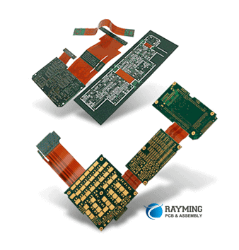
Rigid-flexible printed circuit boards (PCBs), commonly known as flex circuits or flex PCBs, contain both rigid and flexible substrates in a single assembly. They provide solutions for complex interconnections, space and weight savings, and improved reliability compared to traditional rigid boards. 12 layer rigid flex PCBs with multiple rigid and flexible layers enable even higher interconnect density and more complex circuit designs.
This article will provide a comprehensive overview of 12 layer rigid-flex PCBs, including:
- Benefits and applications
- Materials and construction
- Design considerations and guidelines
- Manufacturing processes
- Quality control and testing
- Cost factors
Understanding the intricacies of these advanced boards will help you utilize them effectively in your products.
Benefits and Applications of 12 Layer Rigid Flex PCBs
Some key advantages of 12 layer rigid-flex boards:
- High interconnect density: With up to 12 conductive layers, complex circuits with thousands of traces can be designed. Miniaturization is enabled for compact products.
- Flexibility: Dynamic flexing segments allow three-dimensional configurations and motion. Useful for products with moving parts or specialized form factors.
- Reliability: Flexible sections absorb stresses and vibrations instead of transmitting them to solder joints. This improves fatigue life.
- Weight and space savings: Eliminates connectors and allows dense cabling which reduces size and weight.
These benefits make 12 layer rigid-flex PCBs suitable for:
- Consumer electronics – Cell phones, laptops, tablets, wearables
- Automotive electronics – Sensors, cameras, infotainment systems
- Medical devices – Endoscopes, hearing aids, implantables
- Industrial electronics – Robotics, instrumentation, control systems
- Aerospace and defense – Avionics, radars, guidance systems
In short, they are ideal for miniaturized products with complex, high-density circuitry and interconnections. The combination of rigid and flexible materials in one assembly provides packaging and reliability enhancements.
12 Layer Rigid Flex PCB Materials and Construction
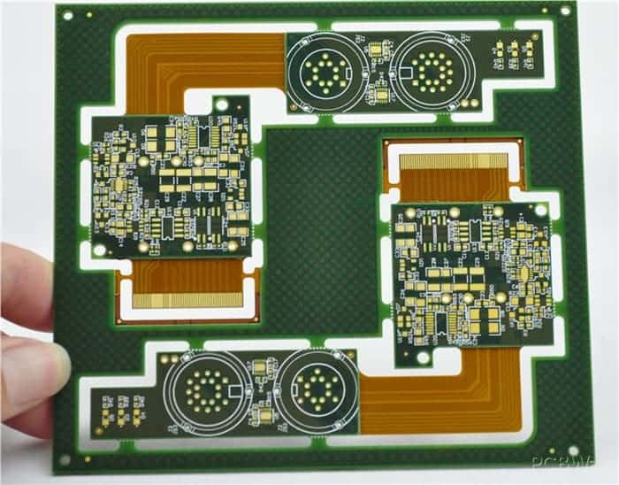
12 layer rigid flex boards contain both rigid and flexible substrates which are laminated together into a multilayer configuration.
Rigid Layers
The rigid sections are typically made from standard FR-4 material which consists of a woven glass fiber reinforcement with an epoxy resin binder. FR-4 provides mechanical strength and stability for the rigid regions of the PCB while allowing high density trace routing and vias.
Common thicknesses range from 0.4mm to 2mm. Thinner rigid layers enable further miniaturization.
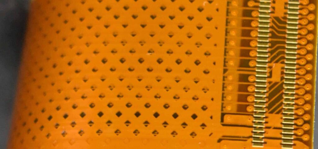
Flexible Layers
The flexible layers provide dynamic bendability to the circuit and are made from polyimide films like Kapton or Upilex. These films have high tensile strength, cut-through resistance, and heat tolerance.
Flex layer thickness is typically 0.05mm to 0.15mm. Thinner material allows tighter bend radii.
Bonding Process
The rigid and flexible layers are bonded together using adhesive films like acrylic, epoxy, or polyimide. Thermo-compression bonding laminates the stack up under heat and pressure. Anticorrosive treatments are applied during bonding to increase reliability.
Here is a cross-section showing a typical 12 layer rigid-flex construction:
This combination of multiple rigid and flexible layers provides design flexibility to route traces for high-density interconnections.
Design Considerations for 12 Layer Rigid Flex PCBs
Careful design is essential to maximize the benefits while avoiding issues during fabrication and assembly of 12 layer rigid-flex boards.
Layer Stack Planning
- Plan position and layout of rigid and flex sections based on interconnect requirements and product assembly. Get board house input.
- Minimize number of layer transitions between rigid and flex areas. This reduces complexity.
- Balance number of layers in rigid and flex sections. Avoid big differences in layer counts.
- Maintain symmetry throughout the stackup to avoid warpage. Alter glass styles if needed.
- Add dummy metal layers if necessary to maintain symmetry in flex areas.
Trace Routing
- Use wide traces and spacing in flex sections for better dynamic bend performance.
- Avoid 90?? traces in high flex areas. Use arcs and zigzag routing instead.
- Plan routing to avoid traces crossing over cutouts or slit regions for rigid-flex transitions.
Component Placement
- Position components in rigid sections, avoid placing on flex areas.
- Distribute component weight evenly to avoid stress imbalances. Watch for dense areas.
- Watch component heights to ensure sufficient clearance in flexed state.
Board Outline and Cutouts
- Use minimum 2mm width tabs when dividing rigid sections with cutouts and slits. Avoid hairline cuts.
- Allow ~3-5X bend radius for flex corners along the board outline. Avoid sharp corners.
- Radius flex section edges to reduce potential cracks from flexing stress.
Vias
- Fill vias in flex areas for reliability. Avoid unfilled vias which collect moisture and crack.
- Avoid via stacks in highly flexed regions. Use staggered vias instead.
Stiffeners
- Use stiffeners and bondply layers to provide mechanical strength and prevent warpage.
- Place stiffeners strategically, such as along board edges or around cutouts.
Text Marking
- Avoid silkscreen or soldermask text on flexible areas which will crack. Use the rigid areas.
Flex and Assembly
- Build in proper strain relief for flexed traces entering soldered connectors.
- Design guide features like bosses to control and constrain flex bending.
Manufacturing Processes for 12 Layer Rigid Flex PCBs
Fabricating complex 12 layer rigid-flex boards requires specialized manufacturing techniques and precautions.
Image Transfer
Photolithography and etching processes transfer the circuit pattern onto each individual dielectric layer. Maintaining fine line resolution and registration across 12 layers requires advanced imaging systems.
Layer Alignment and Registration
The layers must be precisely aligned to ensure vias and traces connect accurately between layers during lamination. Equipment such as laser direct imaging (LDI) greatly improves alignment precision compared to standard methods.
Layer Preparation
Surface treatments enhance adhesive bonding between the layers. Chemical processes create micro-roughened surfaces on the dielectric materials and apply bond-promoting coatings.
Layer Lamination
The treated individual cores are stacked in the proper sequence and bonded together under heat and pressure. The laminate cures into a complete board with the required number of conductive layers separated by dielectric.
Etching and Outer Layer Imaging
The outer layer conductors are formed by etching away unwanted copper after applying a temporary etch resist image. Photolithography transfers the fine line etching pattern.
Solder Masking
The solder mask coats provides insulation and protects etched conductors. LPI (liquid photo-imageable) mask offers high resolution. Special flex formulations avoid cracking.
Final Metallization
Finished outer layer traces are coated with immersion gold, ENIG, or OSP for oxidation protection and solderability.
Singulation
The large laminated panel is divided into individual PCBs. Complex rigid-flex shapes with tight tolerances are cut using precise router equipment.
Quality Control
At each process stage, parameters like alignment, lamination quality, trace defects, and isolation are verified before proceeding. Automated optical inspection (AOI) and other testing ensures repeatable quality.
Quality Control and Testing
To guarantee reliability of the finished 12 layer rigid flex boards, they undergo rigorous inspection and testing:
Appearance Inspection
- Verify trace definition, spacing, continuity, and acceptable pad shapes.
- Check for surface defects like scratches, nicks, spots, and discoloration.
- Detect drilling issues – hole quality, spacing, alignment.
- Flexible area inspection – look for cracks, retained fibers, adhesive voids.
Dimensional Metrology
- X-ray and ultrasonic inspection of inner layers before lamination.
- Measure features like trace width/spacing, hole sizes, outline dimensions.
- Check layer alignment and resist coating qualities.
- Measure thickness of individual layers and total board thickness.
Electrical Testing
- Test for opens, shorts, and impedance faults.
- Continuity check of circuits and vias with flying probe or bed-of-nails test.
- Verify insulation resistance.
- Monitor impedance of critical traces.
- Functional testing of circuits prior to shipment.
Reliability Testing
- Solderability testing to IPC standards verifies pad wetting.
- Environmental stress tests – temperature cycling, vibration, humidity/bias.
- Flex cycling under bending loads checks for flex cracks.
- Condition new boards prior to assembly to prevent assembly failures.
Rigid functional testing combined with dynamic flex tests ensures the complex boards will perform reliably in service.
Cost Considerations for 12 Layer Rigid Flex PCBs
Here are key pricing factors to consider for 12 layer rigid-flex PCBs:
- Number of conductive layers – Each additional metal layer increases fabrication complexity and cost. Balance layer count with density needs.
- Flex vs Rigid area ratio – More flexible area requires additional specialized processing. Aim for under 30% flex area if possible.
- Dielectric materials – Base materials plus adhesive films. More exotic flex materials add cost.
- Number of discrete rigid sections – Each rigid “island” requires precision contouring. Simplify board outline if feasible.
- Line width/spacing – Tighter trace resolution and spacing increases imaging demands and tolerances.
- Registration and tolerances – Holding tighter alignment across 12 layers adds cost.
- Design complexity – More cutouts, irregular board shape, etc. adds fabrication steps.
- Testing requirements – Advanced inspection, measurement tools, reliability tests add cost.
- Order quantity – Higher quantities provide economy of scale benefits.
Work closely with your PCB supplier to optimize cost through design choices and achieve the right balance of capability, quality, and affordability.
Frequently Asked Questions
What are the main advantages of 12 layer rigid flex PCBs compared to traditional rigid boards?
The combination of multiple rigid and flexible layers in one assembly provides several key benefits over rigid PCBs:
- Greater interconnect density through more routing layers
- Flexible sections for three-dimensional configurations
- Dynamic flexing absorbs vibration and shock
- Eliminates connectors and reduces weight
- Enables miniaturization and innovative packaging
What are some examples of products that use 12 layer rigid flex PCBs?
Some common applications are:
- Laptops, tablets, cell phones
- Servers, network switches
- Medical endoscopes, implants
- Automotive electronics
- Aerospace avionics
- Industrial robotics
- High density wearable devices
The boards are ideal when the product needs to be compact and lightweight with reliable complex circuits.
What are the typical dielectric materials used in 12 layer rigid flex PCBs?
The rigid sections use FR-4 material – fiberglass reinforced epoxy laminates. The flexible layers are polyimide films such as Kapton or Upilex. Bonding films are usually acrylic or polyimide adhesives. Specialty materials can also be used.
What are some best practices to follow when designing 12 layer rigid flex PCBs?
Some key guidelines include:
- Minimize layer transitions between rigid and flex sections
- Balance layer counts throughout the stackup
- Use wider traces/spacing in flex areas
- Avoid vias in highly dynamic flex sections
- Distribute components evenly, keep them in rigid sections
- Use minimum 2mm tabs around cutouts
- Allow sufficient corner radii for flexible areas
- Incorporate stiffeners and bondply layers
Following design rules and fabricator recommendations helps avoid manufacturability issues.
What are some of the most important tests conducted on 12 layer rigid flex PCBs?
Critical quality control and reliability tests include:
- Dimensional inspection – features, layer alignment, thickness
- Electrical testing – shorts, opens, continuity, impedance
- Functional circuit testing
- Flex cycling under bending loads
- Environmental stress testing – temperature, vibration, humidity
- Solderability testing
The combination of electrical, mechanical, and environmental tests helps ensure the boards will function reliably over their operating lifetime.


Leave a Reply