Introduction to PCB Stack-Up
Printed Circuit Board (PCB) stack-up refers to the arrangement of copper layers and insulating materials that make up a PCB. The stack-up determines the electrical properties, mechanical strength, and manufacturability of the board. In this article, we will focus on the 12 layer PCB stack-up and its associated thickness.
Why is PCB Stack-Up Important?
PCB stack-up is crucial for several reasons:
-
Signal Integrity: The arrangement of layers affects the signal integrity of the board. Proper stack-up design minimizes crosstalk, reduces electromagnetic interference (EMI), and ensures reliable signal transmission.
-
Impedance Control: The stack-up influences the characteristic impedance of the traces. Maintaining consistent impedance is essential for high-speed designs to prevent signal reflections and distortions.
-
Power Distribution: The placement of power and ground planes in the stack-up impacts the power distribution network. Optimal positioning minimizes voltage drop and ensures stable power delivery to components.
-
Manufacturability: The stack-up affects the manufacturability of the PCB. Proper design considerations, such as the number of layers, layer spacing, and via placement, contribute to a smoother fabrication process.
12 Layer PCB Stack-Up
A 12 layer PCB stack-up is a complex arrangement that offers enhanced functionality and performance compared to simpler stack-ups. It is commonly used in high-density designs, such as telecommunications equipment, networking devices, and aerospace applications.
Typical 12 Layer PCB Stack-Up Configuration
Here is a typical 12 layer PCB stack-up configuration:
| Layer | Material | Thickness (mm) |
|---|---|---|
| Top Solder Mask | Solder Mask | 0.025 |
| Top Copper (Layer 1) | Copper | 0.035 |
| Prepreg | FR-4 | 0.180 |
| Inner Copper (Layer 2) | Copper | 0.017 |
| Core | FR-4 | 0.150 |
| Inner Copper (Layer 3) | Copper | 0.017 |
| Prepreg | FR-4 | 0.180 |
| Inner Copper (Layer 4) | Copper | 0.017 |
| Core | FR-4 | 0.300 |
| Inner Copper (Layer 5) | Copper | 0.017 |
| Prepreg | FR-4 | 0.180 |
| Inner Copper (Layer 6) | Copper | 0.017 |
| Core | FR-4 | 0.300 |
| Inner Copper (Layer 7) | Copper | 0.017 |
| Prepreg | FR-4 | 0.180 |
| Inner Copper (Layer 8) | Copper | 0.017 |
| Core | FR-4 | 0.300 |
| Inner Copper (Layer 9) | Copper | 0.017 |
| Prepreg | FR-4 | 0.180 |
| Inner Copper (Layer 10) | Copper | 0.017 |
| Core | FR-4 | 0.150 |
| Inner Copper (Layer 11) | Copper | 0.017 |
| Prepreg | FR-4 | 0.180 |
| Bottom Copper (Layer 12) | Copper | 0.035 |
| Bottom Solder Mask | Solder Mask | 0.025 |
The total thickness of this 12 layer PCB stack-up is approximately 2.537 mm (99.9 mils).
Layer Functionality
In a 12 layer PCB stack-up, each layer serves a specific purpose:
-
Layers 1 and 12: These are the top and bottom layers of the PCB, respectively. They are used for component placement, routing, and forming solder connections.
-
Layers 2, 4, 6, 8, 10: These are the inner signal layers used for routing traces between components. They are arranged symmetrically to maintain signal integrity and minimize warpage.
-
Layers 3, 5, 7, 9, 11: These layers are typically used as power or ground planes. They provide a low-impedance path for power distribution and help reduce EMI.
Design Considerations
When designing a 12 layer PCB stack-up, several factors should be considered:
-
Layer Spacing: The spacing between layers should be carefully chosen to achieve the desired impedance and minimize crosstalk. The dielectric constant and thickness of the insulating material (e.g., FR-4) play a crucial role in determining the spacing.
-
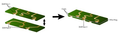
Via Placement: Vias are used to interconnect different layers of the PCB. Proper via placement is essential to minimize signal integrity issues and ensure manufacturability. Blind and buried vias can be used to optimize the routing and reduce the overall board size.
-
Copper Weight: The copper weight (thickness) of each layer should be selected based on the current carrying requirements and the desired trace width. Thicker copper layers are used for power planes and high-current traces, while thinner layers are suitable for signal routing.
-
Impedance Control: To maintain consistent impedance throughout the board, the stack-up should be designed with controlled impedance in mind. This involves selecting the appropriate dielectric materials, copper weights, and trace geometries.

PCB Thickness Considerations
The thickness of a 12 layer PCB is an important factor that affects its mechanical strength, thermal management, and overall performance.
Factors Affecting PCB Thickness
Several factors contribute to the overall thickness of a 12 layer PCB:
-
Layer Count: The number of layers directly influences the thickness of the board. Each additional layer adds to the total thickness.
-
Copper Weight: The thickness of the copper layers affects the overall PCB thickness. Thicker copper layers increase the board thickness.
-
Insulating Material: The choice of insulating material (e.g., FR-4) and its thickness impact the total thickness of the PCB.
-
Solder Mask: The presence of solder mask on the top and bottom layers adds to the overall thickness.
Thickness Tolerance
PCB fabrication involves various processes, and each process introduces some level of thickness variation. It is essential to specify the acceptable thickness tolerance when designing a 12 layer PCB.
Typical thickness tolerance for a 12 layer PCB is ±10% of the nominal thickness. For example, if the nominal thickness is 2.537 mm, the acceptable range would be 2.283 mm to 2.791 mm.
Thickness and Mechanical Strength
The thickness of a 12 layer PCB directly affects its mechanical strength. Thicker boards are generally more rigid and resistant to bending and warping. However, increasing the thickness beyond a certain point may lead to diminishing returns in terms of mechanical strength.
It is important to strike a balance between the required mechanical strength and the constraints of the design, such as space limitations and weight requirements.

Frequently Asked Questions (FAQ)
- What is the typical thickness of a 12 layer PCB?
-
The typical thickness of a 12 layer PCB is around 2.5 mm to 3.0 mm (98 mils to 118 mils). However, the exact thickness depends on factors such as copper weight, insulating material, and solder mask.
-
Can a 12 layer PCB be made thinner?
-
Yes, a 12 layer PCB can be made thinner by using thinner copper layers, selecting thinner insulating materials, and optimizing the stack-up configuration. However, reducing the thickness may impact the mechanical strength and signal integrity of the board.
-
How does the stack-up affect signal integrity in a 12 layer PCB?
-
The stack-up of a 12 layer PCB affects signal integrity in several ways. The arrangement of signal, power, and ground layers influences crosstalk, EMI, and impedance control. Proper stack-up design, including layer spacing and via placement, helps minimize signal integrity issues.
-
What are the advantages of using a 12 layer PCB?
-
The advantages of using a 12 layer PCB include increased routing density, improved signal integrity, better power distribution, and enhanced mechanical strength. It allows for more complex designs and higher performance compared to boards with fewer layers.
-
How does the thickness of a 12 layer PCB affect its manufacturability?
- The thickness of a 12 layer PCB can affect its manufacturability in terms of drilling, plating, and lamination processes. Thicker boards may require specialized equipment and longer processing times. It is important to consider the manufacturability aspects when designing the stack-up and specifying the thickness tolerance.

Conclusion
The 12 layer PCB stack-up and thickness are critical aspects of PCB design that impact the electrical performance, mechanical strength, and manufacturability of the board. Understanding the typical stack-up configuration, layer functionality, and design considerations is essential for creating reliable and high-performance 12 layer PCBs.
By carefully selecting the appropriate layer arrangement, materials, and thicknesses, designers can optimize signal integrity, power distribution, and mechanical properties while ensuring manufacturability. Collaborating closely with PCB fabricators and considering their capabilities and limitations is crucial for successful 12 layer PCB design and fabrication.
As technology advances and demands for higher density and performance increase, the complexity of 12 layer PCBs will continue to grow. Staying updated with the latest design techniques, materials, and manufacturing processes will be essential for engineers and designers working on these complex boards.


Leave a Reply