1. Inadequate Design and Documentation
Causes of Design and Documentation Issues
One of the primary reasons for PCB Manufacturing Defects is inadequate design and documentation. Poor design practices, incomplete specifications, and unclear documentation can lead to misinterpretation and errors during the manufacturing process. Common design and documentation issues include:
- Incorrect or missing component footprints
- Inadequate clearance between components and traces
- Inconsistent or ambiguous labeling
- Lack of detailed assembly instructions
Solutions to Mitigate Design and Documentation Issues
To eliminate PCB manufacturing defects caused by design and documentation issues, consider the following best practices:
- Use industry-standard CAD tools for PCB design
- Follow established design guidelines and rules
- Conduct thorough design reviews and validation
- Provide clear and comprehensive documentation, including bill of materials (BOM), assembly drawings, and test specifications
- Collaborate closely with the manufacturing team to ensure clarity and alignment
2. Incorrect Material Selection
Importance of Material Selection
The choice of materials used in PCB manufacturing plays a crucial role in the overall quality and performance of the final product. Incorrect material selection can lead to various issues, such as:
- Incompatibility with the intended application environment
- Reduced electrical performance and signal integrity
- Decreased mechanical strength and durability
- Increased susceptibility to thermal and mechanical stress
Factors to Consider When Selecting Materials
To avoid PCB manufacturing defects caused by incorrect material selection, consider the following factors:
- Electrical properties: Dielectric constant, dissipation factor, and insulation resistance
- Thermal properties: Glass transition temperature (Tg), coefficient of thermal expansion (CTE), and thermal conductivity
- Mechanical properties: Flexural strength, tensile strength, and elongation
- Environmental factors: Temperature range, humidity, and chemical resistance
- Cost and availability of materials

3. Improper Handling and Storage
Impact of Handling and Storage on PCB Quality
Improper handling and storage of PCBs and components can introduce defects and compromise the integrity of the final product. Common issues related to handling and storage include:
- Exposure to moisture, dust, and contaminants
- Physical damage due to mishandling or improper packaging
- Electrostatic discharge (ESD) damage to sensitive components
- Degradation of materials due to prolonged storage or exposure to extreme conditions
Best Practices for PCB Handling and Storage
To minimize PCB manufacturing defects caused by improper handling and storage, follow these best practices:
- Implement ESD protection measures, such as grounded workstations and personal grounding straps
- Use appropriate packaging materials, such as moisture barrier bags and antistatic containers
- Store PCBs and components in a controlled environment with regulated temperature and humidity
- Follow proper handling procedures, such as using gloves and avoiding excessive bending or twisting of the boards
- Implement a first-in, first-out (FIFO) inventory management system to avoid prolonged storage

4. Soldering Defects
Types of Soldering Defects
Soldering is a critical process in PCB manufacturing, as it establishes electrical connections between components and the board. Soldering defects can lead to various issues, such as:
- Cold joints: Insufficient heat or improper soldering technique resulting in weak and brittle connections
- Bridging: Excess solder creating unintended connections between adjacent pads or traces
- Insufficient wetting: Inadequate solder coverage on the pad or component lead
- Tombstoning: One end of a surface mount component lifting off the pad due to uneven heating or solder paste application
Strategies to Eliminate Soldering Defects
To minimize soldering defects in PCB manufacturing, consider the following strategies:
- Use appropriate soldering techniques, such as reflow soldering for surface mount components and wave soldering for through-hole components
- Optimize soldering parameters, including temperature profile, preheating, and cooling rates
- Ensure proper solder paste application using stencils or automated dispensing systems
- Implement automated optical inspection (AOI) to detect and correct soldering defects early in the process
- Provide adequate training and supervision for manual soldering operations

5. Contamination and Cleanliness Issues
Sources of Contamination in PCB Manufacturing
Contamination and cleanliness issues can introduce defects and affect the reliability of PCBs. Common sources of contamination include:
- Residual flux or solder paste
- Dust, debris, and foreign particles
- Oils, greases, and fingerprints from handling
- Chemical residues from cleaning agents or etching processes
Importance of Maintaining Cleanliness Standards
Maintaining high cleanliness standards throughout the PCB manufacturing process is essential to prevent defects and ensure optimal performance. Benefits of proper cleanliness include:
- Improved electrical insulation and reduced leakage currents
- Enhanced solder joint reliability and mechanical strength
- Reduced risk of corrosion and electrochemical migration
- Improved adhesion of conformal coatings and potting compounds
Cleanliness Control Measures
To control contamination and maintain cleanliness standards in PCB manufacturing, consider the following measures:
- Implement clean room protocols and procedures
- Use appropriate cleaning agents and processes, such as aqueous cleaning or vapor degreasing
- Monitor contamination levels using ionic contamination testing or surface insulation resistance (SIR) testing
- Implement strict handling and storage procedures to minimize exposure to contaminants
- Conduct regular audits and inspections to ensure compliance with cleanliness standards
6. Copper Etching and Plating Defects
Importance of Copper Etching and Plating
Copper etching and plating are critical processes in PCB manufacturing that define the conductive traces and pads on the board. Defects in these processes can lead to issues such as:
- Over-etching or under-etching of traces
- Incomplete or uneven plating
- Lifting or peeling of copper traces
- Reduced electrical conductivity and signal integrity
Causes of Copper Etching and Plating Defects
Copper etching and plating defects can occur due to various factors, including:
- Incorrect etching or plating parameters, such as time, temperature, and chemical concentrations
- Contamination of the etching or plating solutions
- Inadequate surface preparation or cleaning
- Mechanical stress or damage during handling
Strategies to Minimize Copper Etching and Plating Defects
To minimize copper etching and plating defects in PCB manufacturing, consider the following strategies:
- Optimize etching and plating parameters through process control and monitoring
- Regularly maintain and replace etching and plating solutions to ensure consistency and purity
- Implement strict cleanliness and contamination control measures
- Use automated handling systems to minimize mechanical stress and damage
- Conduct regular visual and electrical inspections to detect and correct defects early in the process
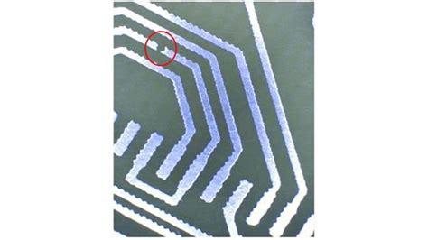
7. Drill and Hole Defects
Types of Drill and Hole Defects
Drill and hole defects are common issues in PCB manufacturing that can affect the mechanical and electrical integrity of the board. Common types of drill and hole defects include:
- Misaligned or mislocated holes
- Oversized or undersized holes
- Burrs or rough hole edges
- Smearing or debris in the holes
- Incomplete or missing plating in the holes
Causes of Drill and Hole Defects
Drill and hole defects can occur due to various factors, such as:
- Incorrect drill bit selection or wear
- Improper drilling parameters, such as feed rate and spindle speed
- Inadequate workpiece clamping or support
- Contamination or debris on the drill bit or workpiece
- Incorrect plating or deburring processes
Strategies to Eliminate Drill and Hole Defects
To eliminate drill and hole defects in PCB manufacturing, consider the following strategies:
- Use high-quality and properly maintained drill bits
- Optimize drilling parameters based on the material and hole size
- Implement robust workpiece clamping and support systems
- Regularly clean and inspect drill bits and workpieces
- Use appropriate plating and deburring processes to ensure hole quality and reliability
8. Solder Mask and Silkscreen Defects
Importance of Solder Mask and Silkscreen
Solder mask and silkscreen are essential features in PCB manufacturing that provide insulation, protection, and identification for the board. Defects in these areas can lead to various issues, such as:
- Inadequate insulation and increased risk of short circuits
- Poor adhesion and durability of the solder mask
- Incorrect or illegible component markings
- Cosmetic defects that affect the appearance and brand image
Causes of Solder Mask and Silkscreen Defects
Solder mask and silkscreen defects can occur due to several factors, including:
- Incorrect application or curing of the solder mask or silkscreen ink
- Contamination or debris on the board surface
- Incompatibility between the solder mask and the base material
- Improper artwork or design files
- Mechanical damage during handling or processing
Strategies to Minimize Solder Mask and Silkscreen Defects
To minimize solder mask and silkscreen defects in PCB manufacturing, consider the following strategies:
- Use high-quality and compatible solder mask and silkscreen materials
- Optimize the application and curing processes for consistent and reliable results
- Ensure proper surface cleaning and preparation before application
- Verify artwork and design files for accuracy and completeness
- Implement gentle handling and processing techniques to avoid mechanical damage
9. Inadequate Testing and Inspection
Importance of Testing and Inspection in PCB Manufacturing
Testing and inspection are critical steps in PCB manufacturing that ensure the quality, functionality, and reliability of the final product. Inadequate testing and inspection can lead to various issues, such as:
- Undetected defects and failures
- Reduced yield and increased rework costs
- Delayed product delivery and customer dissatisfaction
- Potential field failures and warranty claims
Types of Testing and Inspection in PCB Manufacturing
PCB manufacturing involves various types of testing and inspection, including:
- Visual inspection: Manual or automated inspection of the board for visible defects, such as scratches, discoloration, or missing components
- Automated Optical Inspection (AOI): Automated inspection using cameras and image processing algorithms to detect defects, such as misaligned components or solder bridges
- X-ray inspection: Non-destructive inspection using X-rays to detect hidden defects, such as voids, cracks, or missing solder joints
- Electrical testing: Testing the electrical performance and functionality of the board, such as continuity, insulation resistance, and signal integrity
- Functional testing: Testing the board under actual operating conditions to verify its functionality and performance
Strategies to Improve Testing and Inspection Effectiveness
To improve the effectiveness of testing and inspection in PCB manufacturing, consider the following strategies:
- Implement a comprehensive testing and inspection plan that covers all critical aspects of the board
- Use advanced testing and inspection equipment, such as AOI machines and X-ray systems
- Establish clear acceptance criteria and quality standards for each testing and inspection stage
- Provide adequate training and resources for the testing and inspection personnel
- Conduct regular audits and reviews to identify areas for improvement and ensure compliance with quality standards
10. Insufficient Process Control and Monitoring
Importance of Process Control and Monitoring
Process control and monitoring are essential aspects of PCB manufacturing that ensure consistency, repeatability, and quality throughout the production process. Insufficient process control and monitoring can lead to various issues, such as:
- Inconsistent quality and performance of the final product
- Increased defect rates and rework costs
- Difficulty in identifying and correcting root causes of defects
- Reduced efficiency and productivity of the manufacturing process
Key Elements of Process Control and Monitoring
Effective process control and monitoring in PCB manufacturing involves several key elements, including:
- Establishing clear process parameters and control limits for each manufacturing stage
- Implementing sensors, gauges, and data acquisition systems to collect real-time process data
- Using statistical process control (SPC) techniques to analyze process data and identify trends or anomalies
- Implementing corrective and preventive actions (CAPA) to address process deviations and improve performance
- Conducting regular process audits and reviews to ensure compliance and identify opportunities for improvement
Strategies to Enhance Process Control and Monitoring
To enhance process control and monitoring in PCB manufacturing, consider the following strategies:
- Invest in advanced process control and monitoring technologies, such as real-time data acquisition systems and SPC software
- Establish a robust quality management system (QMS) that defines process parameters, control limits, and performance metrics
- Provide training and resources for the manufacturing personnel to understand and implement process control and monitoring techniques
- Foster a culture of continuous improvement and encourage employee participation in identifying and solving process issues
- Collaborate with suppliers and customers to align process control and monitoring practices and ensure end-to-end quality
FAQ
- What are the most common PCB manufacturing defects?
-
Some of the most common PCB manufacturing defects include soldering defects, drill and hole defects, copper etching and plating defects, and solder mask and silkscreen defects.
-
How can inadequate design and documentation lead to PCB manufacturing defects?
-
Inadequate design and documentation can lead to misinterpretation and errors during the manufacturing process, resulting in issues such as incorrect component placement, inadequate clearance, and inconsistent labeling.
-
Why is material selection important in PCB manufacturing?
-
Material selection is crucial in PCB manufacturing because it affects the electrical, thermal, and mechanical properties of the board, as well as its compatibility with the intended application environment and manufacturing processes.
-
What are the consequences of improper handling and storage of PCBs and components?
-
Improper handling and storage can introduce defects and compromise the integrity of PCBs and components, leading to issues such as moisture exposure, physical damage, electrostatic discharge (ESD) damage, and material degradation.
-
How can process control and monitoring help in reducing PCB manufacturing defects?
- Process control and monitoring help in ensuring consistency, repeatability, and quality throughout the PCB manufacturing process by establishing clear process parameters, collecting real-time data, analyzing trends, and implementing corrective and preventive actions to address deviations and improve performance.
| Defect Category | Common Causes | Prevention Strategies |
|---|---|---|
| Design and Documentation | – Incorrect or missing component footprints – Inadequate clearance between components and traces – Inconsistent or ambiguous labeling |
– Use industry-standard CAD tools – Follow established design guidelines and rules – Conduct thorough design reviews and validation |
| Material Selection | – Incompatibility with the intended application environment – Reduced electrical performance and signal integrity – Decreased mechanical strength and durability |
– Consider electrical, thermal, mechanical, and environmental properties – Evaluate cost and availability of materials – Consult with material experts and suppliers |
| Handling and Storage | – Exposure to moisture, dust, and contaminants – Physical damage due to mishandling or improper packaging – Electrostatic discharge (ESD) damage to sensitive components |
– Implement ESD protection measures – Use appropriate packaging materials – Store PCBs and components in a controlled environment |
| Soldering Defects | – Cold joints – Bridging – Insufficient wetting – Tombstoning |
– Use appropriate soldering techniques – Optimize soldering parameters – Ensure proper solder paste application – Implement automated optical inspection (AOI) |
| Contamination and Cleanliness | – Residual flux or solder paste – Dust, debris, and foreign particles – Oils, greases, and fingerprints from handling |
– Implement clean room protocols and procedures – Use appropriate cleaning agents and processes – Monitor contamination levels using testing methods |
By understanding the common causes of PCB manufacturing defects and implementing effective prevention strategies, manufacturers can significantly reduce the occurrence of defects and improve the overall quality and reliability of their products. Regular process audits, employee training, and continuous improvement initiatives are also essential for maintaining high standards in PCB manufacturing.


Leave a Reply