 flexpcb.org
FLEXPCB.ORG / informational
Flex PCB Stackup: Layers, Thickness and Tolerances
Get a Flex PCB Quote ↗Specify every material layer
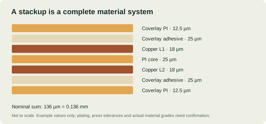
A usable stackup identifies the layer order and the material system, rather than just the number of copper layers. List the copper foil and nominal thickness, dielectric grade, bonding films, coverlay film and coverlay adhesive. Distinguish conductive layers from protective films. Identify where a construction changes across the outline, including exposed contacts, local reinforcement, shielded regions and rigid-flex transitions.
Calculate a nominal thickness before applying tolerances
For an illustrative two-layer construction, use 18 µm copper on each side of a 25 µm PI core, with 12.5 µm coverlay film and 25 µm coverlay adhesive on each face. The nominal sum is 2 × 18 + 25 + 2 × 12.5 + 2 × 25 = 136 µm, or 0.136 mm. These are demonstration values, not a stocked material specification. The stackup builder shows this arithmetic so omitted layers are easier to notice.
Separate nominal values from finished requirements
A nominal material sum is not the same as an inspected finished-thickness specification. Plating, material tolerance, adhesive flow and processing can affect the finished result. Ask the fabricator to state what is included and where thickness is measured. If a connector or housing requires a controlled thickness range, put that range and measurement location on the drawing. Do not convert the builder output into a production tolerance without review.
Keep reinforcement local
If the example flex receives a 200 µm stiffener and an assumed 25 µm attachment adhesive, its reinforced region becomes 136 + 200 + 25 = 361 µm, or 0.361 mm. The unsupported bending region remains 0.136 mm. Specify the reinforcement outline, material and attachment system separately, and confirm the allowed distance from the bend. A stiffener selection in a visual tool does not validate the transition geometry.
Freeze the electrical reference construction
Controlled impedance depends on more than total thickness. Review the signal layer, reference conductor, dielectric properties, copper profile and finished geometry with the fabricator. Agree how the impedance will be modelled and tested before routing is released. Review transitions between regions as part of the signal path. Record the agreed stackup revision in the fabrication package so a material substitution or layer change triggers a deliberate review.
Make the requirements reviewable.
| Define | Include in the review | Why it matters |
|---|---|---|
| Mechanical duty | Installed shape, bend location, motion and cycle target | Distinguishes installation bending from service fatigue |
| Construction | Layer order, copper, film, adhesive and coverlay | Establishes finished thickness and material compatibility |
| Interfaces | Connector thickness, pad finish and local reinforcement | Controls fit, assembly support and contact reliability |
| Acceptance | Dimensions, electrical test and applicable standard revision | Creates an agreed basis for inspection and quotation |
CONTINUE THE DESIGN REVIEW
Connect the decisions.
YOUR NEXT STEP
Bring the requirements.
Start the conversation.
Tell us what the circuit needs to do, how it will bend and when you need it. A complete build brief makes a quote easier to evaluate.
Preparing files?
Include Gerber and drill data, a fabrication drawing and stackup notes. Put related files in one ZIP. Add a BOM and placement file when assembly is required.